
Effect of the Shorting Pin
Shorting of the patch to ground enhances the impedance matching and also introduces a polarization change. The shorting pin acts as an inductance parallel to the resonant LC circuit. When the shorting pin shifts from the center toward the right edge of the patch, the value of the inductance—in series with the static capacitance of the patch in an equivalent circuit of the antenna—increases. This causes the overall input impedance of the antenna to decrease. Impedance matching of the antenna improves28-34 with the pin position in Figure 5a, as observed in Figures 5b and c.
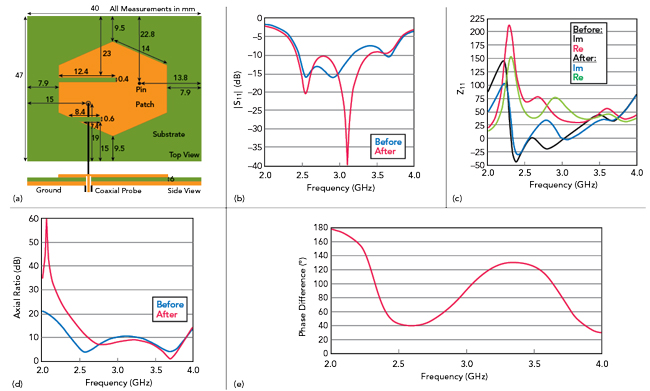
Figure 5 Design with two slits and incorporating a shorting pin (a), showing the effect on |S11| (b), Z11 (c) and axial ratio (d). Phase difference between the TM10 and TM01 modes (e).
Before shorting of the patch to ground, the modified antenna radiates linear polarization over the total resonant band, which is evident from the high axial ratio (see Figure 5d). After shorting the patch, however, the current distribution from 3.63 to 3.77 GHz produces two orthogonal degenerate modes (TM01 and TM10) with the same magnitudes; however, the phase difference between them is not 90 degrees, an essential condition for circular polarization. To satisfy the orthogonality condition, the position of the shorting pin is moved from the center toward the right edge of the patch, so the effective surface current path associated with the TM01 mode is slightly greater in one direction, compared to the TM10 mode in another direction. This causes the TM10 mode resonant frequency to shift slightly higher than the TM01 mode resonance, causing the phase difference of the two modes to equal 90 degrees. The condition required for circular polarization over the 3.63 to 3.77 GHz band is therefore satisfied.35,36 The antenna modified with a shorting pin generates circular polarization from 3.63 to 3.77 GHz and linear polarization in the remaining portion of the operational frequency band.
Axial ratio and phase difference are measures of circular polarization. If the axial ratio is less than 3 dB and the phase difference is around 90 degrees over a frequency range, the antenna is considered to be circularly polarized over that range (see Figures 5d and 5e). To determine the optimum pin position, a parametric simulation using HFSS explored different pin positions on the radiating patch, observing |S11|, input impedance and axial ratio. A pin position of 22.8 mm from the upper edge and 13.8 mm from the right edge of the substrate was found to be optimum.
Effect of a Third Slit
From Figure 5b, the upper end of the 2.4 to 3.69 GHz frequency band has a return loss less than 10 dB due to poor impedance matching. Perturbing the patch with an optimized third slit (see Figure 1) shifts the input impedance closer to 50 Ω (see Figure 6) and improves the impedance match at the upper end of the band.
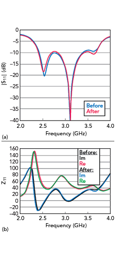
Figure 6 Effect of the third slit on |S11| (a) and Z11 (b).
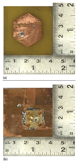
Figure 7 Fabricated antenna top (a) and bottom (b) view.

MEASURED RESULTS
A prototype antenna (see Figure 7) was measured using a Keysight E5071B network analyzer in an anechoic chamber. A comparison of the simulated and measured parameters are shown in Table 3. |S11|, radiation patterns, input impedance and gain with linear and circular polarization are shown in Figures 8 through 13. The measurement results correspond well with the simulations. Still, small differences can be seen, which are attributed to connector soldering and the non-ideal measuring environment, which were not modeled. Figure 12 shows the antenna’s simulated and measured linear polarized co-polarization (Co-pol) and cross-polarization (X-pol) patterns in a 2D plane at 2.5 GHz. Figure 13 shows the simulated and measured right-hand and left-hand circular polarization patterns in a 2D plane at 3.68 GHz.
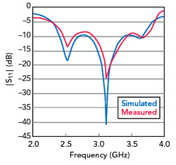
Figure 8 Measured vs. simulated |S11|.
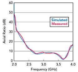
Figure 9 Measured vs. simulated axial ratio.
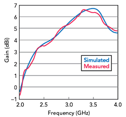
Figure 10 Measured vs. simulated gain.
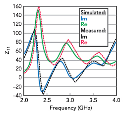
Figure 11 Measured vs. simulated Z11.
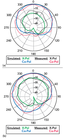
Figure 12 Measured vs. simulated radiation patterns at 2.5 GHz: φ = 0 (a) and φ = 90 (b) degrees.
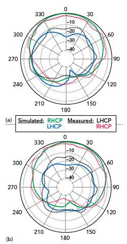
Figure 13 Measured vs. simulated radiation patterns at 3.68 GHz: φ = 0 (a) and φ = 90 (b) degrees.