Radio detection and ranging or RADAR has been around since its first implementation in the early 1900s when the use of radio waves was first used to detect the presence of ships in dense fog. The actual acronym was not coined until the early 1940s. X-band radar, in particular, has been around since the outset of World War II and continues to see extensive use. Typical X-band radar applications include air traffic control, detection of precipitation, speeding traffic and military use. Military uses include detecting and tracking aircraft, ships, missiles and other objects with the intention of harming any of our armed forces protecting our country and its interests. Various types of radar include continuous wave (CW), dual-pole, phased array, pulsed, single-pole and synthetic aperture radar (SAR). Many of the advanced X-band radars used today are typically based on active phased arrays requiring the use of many multiple phase array element sections.
Design and Technology
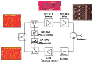
Mimix Broadband is pleased to offer a very competitive and high performance X-band radar phased-array element chip set. Figure 1 shows a typical X-band radar phased-array antenna element block diagram. The transmit portion of the phased-array element includes a 10 W output power amplifier stage (XP1006) specifically designed for pulsed radar applications. The output driver stage (XP1014) is a
1 W MMIC designed to drive the XP1006 device completing the transmit chain. On the receive side of the phased-array element the company will soon be offering a combined low noise amplifier/limiter MMIC that will provide excellent noise figure and high power limiting capability. Lastly, to complete the phased-array element control chain both a wide band attenuator (XA1000) and phase shifter (XS1000) MMIC device are available.
The X-band MMIC chip set uses Mimix Broadband’s six-inch 0.5 μm GaAs PHEMT device model technology and is based on an optical gate lithography to ensure high repeatability and uniformity. Using a 0.5 μm process allows lower cost optical lithography to be used for device deposition and in conjunction with six-inch wafer area provides users with a highly repeatable and lower cost MMIC chip set solution.
All Mimix die products include surface passivation to protect and provide a rugged part with backside vias allowing either a conductive epoxy or eutectic solder die attach process. Most of the company’s products are available in both die and packaged versions, with many provided in RoHS compliant surface-mount packages compatible with high volume solder installation. Both the flanged ceramic and surface-mount packaged amplifiers offer excellent RF and thermal properties.
Power Amplifier
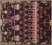
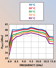
The XP1006 device, shown in Figure 2, is a three-stage 8.5 to 11.0 GHz 10 W power amplifier that has a large-signal gain of 21 dB and provides excellent input/output return loss. Power-added efficiency (PAE) is 30 percent with +40 dBm saturated output power (see Figure 3). This device not only includes on-chip bias circuitry that allows the user to provide a single –5 V bias input but also provides additional gate bias inputs that allow separate gate bias control. All devices are 100 percent wafer probed for RF, DC and output power performance. The power amplifier is offered both in die form and in a soon to be released ceramic flanged package.

Thermal imagery of the XP1006 (see Figure 4) has been taken under various bias conditions using thermal image equipment located at the company’s facility in Houston. Unlike thermal analysis using models to predict thermal resistance, this imager allows Mimix to actually measure channel temperatures of all the devices on the MMIC thus allowing a much more accurate thermal resistance to be determined. Once the thermal resistance has been calculated, reliability information such as mean time to failure (MTTF) and failures in time (FIT) can be calculated allowing more accurate optimal base temperatures to be provided for determining safe operation. An application note describing the usage of the XP1006 in more detail can be found on the company’s web site.
Driver Amplifier

The XP1014 MMIC, shown in Figure 5, is a two-stage 8.5 to 11.0 GHz 1 W power amplifier that has a small-signal gain of 18 dB. Its PAE is 35 percent with +31 dBm saturated output power (see Figure 6). This device includes on-chip bias circuitry that allows the user to provide a single –5 V bias input. As with the previous power amplifier, these devices are 100 percent wafer probed for RF, DC and output power performance as well. They are offered both in die form and in a soon to be released ceramic flanged package.
Attenuator

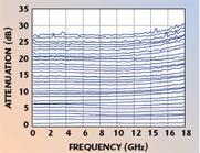
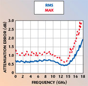
The XA1000 device, shown in Figure 7, is a DC to 18 GHz, five-bit digital attenuator. The device has a 27 dB attenuation range (see Figure 8) with 5.5 dB insertion loss. Its input and output return loss is excellent across all states and the input 1 dB compression point (P1dB) is +24 dBm. Its attenuation error, shown in Figure 9, is less than 1 dB with a phase error of less than 20°. The device is operated using a single –7.5 V supply voltage with five digital binary inputs that meet LVCMOS specifications. All devices are 100 percent wafer probed for RF, DC and attenuation performance. The attenuator is currently offered only in die form with packaged device development starting in the near future.
Phase Shifter

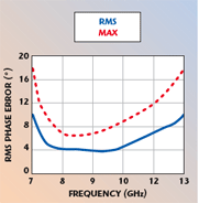
The XS1000 MMIC, shown in Figure 10, is a 7 to 13 GHz, six-bit phase shifter. The device has a LSB of 5.625° (see Figure 11) with 6.5 dB insertion loss. Its input and output return loss is excellent across all states and the input P1dB is +25 dBm. Attenuation error is less than 1 dB with a RMS phase error (shown in Figure 12) of less than 3°. The device is operated using a single 7.5 V supply voltage with six control inputs. All devices are 100 percent wafer probed for RF, DC and phase bit performance. The phase shifter is currently offered only in die form with packaged devices available in 2007.
LNA/Limiter
Lastly are the LNA and limiter functions of the phased-array element. Since radar front ends are susceptible to damage from high input power transmitters, the LNA needs some sort of protection to keep its lower level input devices from being damaged. While there are a number of options that can been chosen, a low loss limiter is typically the best choice for this application. The limiter provides a low insertion loss solution providing the least amount of degradation to front end noise figure but at the same time enough level of input transmit power protection when it is needed to protect the LNA from damage.
The X-band LNA/limiter is still in development at this time and is expected to be available at the end of CY2006. Additional information and its updated status may be obtained from the company’s web site.
Conclusion
A high performance X-band radar phased-array element chip set has been presented that includes driver and power amplifier devices for the transmit side, an LNA/limiter for the receive side, and an attenuator and phase shifter for the control side. The new chip set is fabricated using Mimix Broadband’s six-inch 0.5 mm GaAs PHEMT device model technology and is based on an optical gate lithography process. The new devices represent a highly repeatable, low cost MMIC chip set solution for a radar phased-array element interface. The individual die are surface passivated with backside vias to allow conductive epoxy or eutectic die attach. In addition, the devices are 100 percent RF and DC tested, guaranteeing their performance and allowing users to increase their yields and lower costs.
Devices are now available in die form or in soon to be released ceramic flanged mount and surface-mount packages. Additional information and individual data sheets may be obtained from the company’s web site.

Mimix Broadband Inc.,
Houston, TX (281) 988-4600,
www.mimixbroadband.com
RS No. 300.

