One of the metrics that concern designers is the εreff of a design feature or object. For example, consider a PCB patch array used in an automotive medium to long-range radar at 77 GHz. The tilt of the elevation pattern will vary based on the εreff (see Figure 5). A 1 percent change in the dielectric constant of the patch antenna string is equivalent to a 0.74-degree tilt.

Figure 5 Simulated tilt vs. dielectric constant for a 77 GHz antenna array.
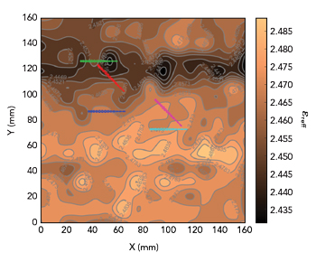
Figure 6 Effective dielectric constant from 16 × 16 measurements across 160 × 160 mm, with a 77 GHz antenna array overlaid in several locations and orientations.
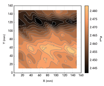
Figure 7 Average effective dielectric constant for the 77 GHz antenna array when placed at 45 degrees anywhere within the measured area.
Any variation based on the designed board can be optimized with one or more prototype builds. Substrate and PCB manufacturing tolerances are known and controlled within a range that can be included in simulations to enable centering the design. However, the controls may not correlate perfectly with what an RF object will experience. Substrate dielectric is measured and controlled by itself, copper foil is controlled by itself and both are spot sampled. PCB manufacturing is controlled by verifying the specific dimensions in discrete locations. But what is the combined variation of the key parameters within a panel?
To evaluate these effects, a 16 × 16 grid of ring resonators were measured on a typical RF substrate, developing a detailed map of the εreff (see Figure 6). The average is 2.47 with variation of ±1.4 percent. An antenna array fabricated on the substrate could be located and oriented anywhere on the panel, as shown in the figure. While each patch in the antenna is small compared to the entire antenna, it could see the range of the effective dielectric constant variation depending on placement. It may be more useful to know the variation in εreff averaged over the entire antenna array. This can be derived by placing the antenna in all possible locations and orientations and calculating the average εeff underneath the array—ideally including significant fringing fields. In this calculation, with the antenna array overlaid at 45 degrees, the average εeff is 2.47 with variation of ±0.9 percent (see Figure 7).
Summarizing, a small feature such as an individual antenna patch at 77 GHz sees the full range of the εreff variation, here 2.47 ±1.4 percent, where the whole antenna string array experiences an average of 2.47 ±0.9 percent. As an entity, the antenna array experiences significantly less variation on average. Similarly, the system variation of εreff for all transmit (Tx) and receive (Rx) antennas combined would be further reduced. The localized variation is a product of all factors, such as localized variation in foil and substrate dielectric, PCB manufacturing processes and board design. Localized, lot-to-lot and panel-to-panel variations and tolerances depend on the specific material and process used, but tolerances will always be present.
Note that the dielectric constant derived from ring resonator measurements may not correspond exactly to the value experienced by an antenna or other circuit. Similarly, any measurement has some tolerance and repeatability. For this experiment, the measurement repeatability was characterized to ±0.3 percent. The averages developed for the mmWave patch antenna discussed here may not fully characterize the variation in performance of another mmWave circuit; nonetheless, the example illustrates the concepts.
When designing an RF system, the manufacturing process must be selected to accommodate system needs, and the material and processing tolerances lot-to-lot, panel-to-panel and within the panel must be considered. Often, there are other system considerations which may impact both the manufacturing process and the resulting tolerances and must be considered. For example, the RFIC can be placed on the antenna side or the opposite side of the PCB.

Figure 8 Via structure (left) for a 76 to 81 GHz layer transition and associated PCB stackup (right).
COMPONENT SOLUTIONS
Conducting signals to different layers using vias is very common. The mismatch introduced by the high impedance of via structures and the parasitic effects of via stubs are significant at mmWave. Stub reduction and additional matching are usually required to compensate, with the performance verified using full 3D electromagnetic (EM) simulation. Manufacturing tolerances of all the parameters should be considered early in design.
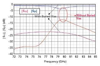
Figure 9 Buried via insertion loss and return loss comparison.
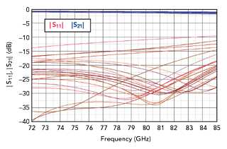
Figure 10 Tolerance study of the layer transition using buried vias.
In many mmWave radars where the frequencies are higher than 60 GHz, the design must prevent radiation from the via structures. A dense ring of ground vias is usually placed around the signal via to provide a ground shield, containing the EM fields inside a quasi-coaxial structure and minimizing radiation loss. However, these ground vias can short the trace and block the signal routing in and out of the center signal via. Figure 8 shows a via structure and its PCB stackup that conducts 76 to 81 GHz signals from the bottom to top layers in an automotive radar. Six plated through holes surrounding the center signal via serve as ground vias. However, they do not provide enough shielding at the upper frequencies, requiring two additional buried vias to close the gap while not shorting the traces. If the buried vias are removed, the insertion loss and return loss degrade significantly (see Figure 9). The tolerance study of the via transition is shown in Figure 10. It includes the manufacturing tolerances of etching, via registration, via diameter and variation of the dielectric material thickness and dielectric constant. Tolerance studies help ensure the RF performance meets system requirements considering all the manufacturing variability.

Figure 11 Layout (left) and simplified PCB stackup (right) of layer transition using SMT crossover component.
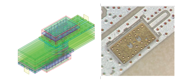
Figure 12 Isometric view (left) and photo (right) of the layer transition using a crossover component.
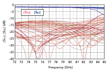
Figure 13 Tolerance analysis of the layer transition using the crossover component.
As discussed, buried vias require additional lamination, drilling and plating, and these additional processes can significantly increase manufacturing cost. A surface mountable (SMT) crossover component can be applied to a single lamination board to achieve the same results, reducing manufacturing complexity (see Figure 11). In this 76 to 81 GHz automotive radar design, only plated through hole vias and micro-vias are used in a common, single lamination stackup. The center signal via and surrounding ground vias are all plated through holes, and micro-vias are placed around the trace for the grounded coplanar waveguide (GCPW) lines. The isolated signal via pad and the end of the GCPW line are not connected by the routings on the PCB; they are bridged together by an SMT crossover component. Mounting the crossover on both top layer and bottom layer, the signal is conducted from the GCPW line on the bottom layer to the GCPW line on the top (see Figure 12). The dimensions of the crossover are about 80 × 50 mil, and the crossover fits nicely with a 10 mil, 50 Ω GCPW line, commonly used for these applications. Since the crossover uses similar mmWave grade PCB substrates and the same multilayer PCB manufacturing processes, the SMT component approach can achieve the same performance and manufacturing process variation as a matched via solution (compare Figure 13 with Figure 10). If a PCB has a low density of such signal transitions, the component solution may offset the added component cost by reducing the board manufacturing cost and yielding an overall price advantage.
SUMMARY
The rapid growth of mmWave applications has created a growing demand for high performance, multilayer PCBs containing mmWave circuitry. Today’s mmWave design requirements can exceed PCB material and process capabilities, as relatively small variations in raw materials and manufacturing processes can degrade the performance of mmWave designs. By incorporating these material and process variations in the design, the desired performance, repeatability and cost in production can be achieved.
