
A key objective when designing radar, electronic warfare and communications systems is to achieve the best range possible within the limited space available. RF GaN technology is best suited to provide the required power density, as well as high temperature and high voltage operation, for demanding applications. In many pulsed radar systems, the carrier frequency of the pulses is constant, but the pulse repetition interval (PRI) and the pulse width vary. A longer PRI and low duty cycle offer better unambiguous measurement range or range resolution. However, lower PRI, higher duty cycle and greater pulse width deliver more power per pulse and, therefore, longer range.
Modern marine and air surveillance radars continually change operating modes by changing PRIs and pulse widths to suit the different requirements of target search, acquisition and tracking. Increasingly, defense and commercial applications prefer multimode radar, adding communication and electronic warfare capabilities to active electronically scanned array (AESA) systems. AESAs with thousands of transmit and receive elements for beam steering add to the power density demand from designs.
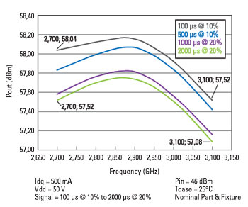
Figure 1 Output power vs. pulse width and duty cycle.
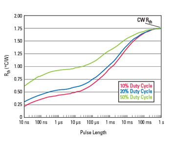
Figure 2 Rth vs. pulse length and duty cycle.
The output power of a GaN HEMT power amplifier (PA) varies with pulse width and duty cycle (see Figure 1). The output power decreases as duty cycle or pulse width increase, assuming everything else in the test remains the same. The effect of duty cycle and pulse width on output power must be considered during the PA design.
THERMAL RESISTANCE
The variation in output power and power-added efficiency reflects the variation in the junction-to-case-thermal resistance, Rθjc, of the RF GaN device with pulse width and duty cycle. Rθjc limits the maximum power dissipation and output power before the device reaches its maximum junction temperature, Tj. Although Rθjc increases with increasing pulse width and duty cycle (see Figure 2), it approaches a fixed value for large pulse widths irrespective of the duty cycle. This ultimate value is the CW thermal resistance.
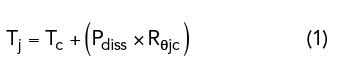
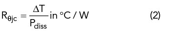
When designing a multimode radar, the correct values of Rθjc must be used, as device reliability or lifetime (mean time to failure), is determined by the power dissipated and resulting junction temperature. The peak junction temperature determines design feasibility and what thermal management solutions are needed. The peak junction temperature is proportional to the case temperature, the dissipated power and the thermal resistance, as given by Equation 1:
To determine Tj, we must determine Rθjc and Pdiss. Thermal resistance (in °C/W) is calculated as the difference in temperature (ΔT in °C) between two surfaces—here the junction and case —that support a fixed <
In Equation (1), Tc can be measured using infrared microscopy; however, measuring Tj to calculate ΔT is more complex. A physical model created using a software tool such as ANSYS and a finite element method simulation is used to correlate the case temperature measurement to the junction temperature.
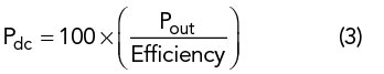
To find Pdiss it is necessary to calculate Pdc:
and from this:

Calculate the peak junction temperature by inserting these values into Equation (1).
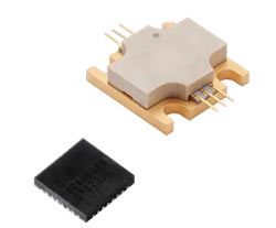
QFN MOUNTING OPTIONS
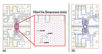
Figure 3 Via array (a) and embedded Cu coin (b) thermal paths.
Designers often choose surface-mount packages such as QFN because they result in a compact PA stage. However, these are typically designed for applications with pulse widths between 100 and 500 µs and duty cycles less than 20 percent. The trend toward multimode and longer pulse operation increases the power dissipation, requiring consideration of package constraints to ensure adequate thermal management.
A common thermal solution for QFNs has been using plated-through vias filled with conductive epoxy that connect the top-surface device mounting layer through the RF ground layer to the chassis (see Figure 3). Via arrays are typically used for power dissipation up to 30 W, with pulse widths under 500 μs and duty cycles less than 20 percent. A high density of vias is needed to dissipate the additional heat generated by new, longer pulse radar designs. Another option is to use a Cu coin embedded in the printed circuit board (PCB). While this may require a thicker multi-layer board to support the coin, with higher processing cost, it performs significantly better thermally for long pulse designs that approach CW (see Figure 2).
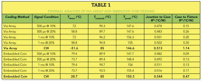
Using the same device with a fixed Pdiss, thermal simulations were run using the via array and embedded coin board designs. In both cases, while the device thermal resistance is independent of the device mounting configuration, the case-to-fixture thermal resistance is not. Table 1 shows a remarkable difference in the fixture temperature, Tfixture, needed to achieve a desired case temperature, Tcase. To maintain Tcase = 85°C with a CW signal, the via array requires an unrealistic fixture temperature of –52°C, compared to 29°C with the embedded Cu coin.
For high-power aerospace and defense applications, metal-ceramic packages that can be mounted directly on the heatsink are recommended. The device thermal resistance, Rth, of the ceramic package is higher than that of the surface-mount option. Unlike metal-ceramic packages, SMT options require the PCB to be included in the thermal path. Since the PCB thermal resistance could be of the same order as the device, it can add a significant temperature differential to the cooling requirements.
PAs FOR RADAR
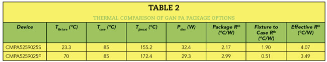
Wolfspeed offers a 25 W GaN MMIC PA for radar systems in the 5.2 to 5.9 GHz range. The 28 V PA is available in both 5 x 5 plastic QFN (CMPA5259025S) and 440219 metal-ceramic flange (CMPA5259025F) packages. To maintain the same 85°C case temperature, the fixture temperature should be 23°C for the QFN “S” model and 70°C for the metal-ceramic “F” model (see Table 2).
Wolfspeed
Durham, N.C.
www.wolfspeed.com/products/rf/