Multi-Chip Modules (MCMs)
Though on-chip integration of CMOS and GaN or GaAs may be futuristic, current advancements have enabled MCM integration of GaN and GaAs.10,11 Where GaN is better suited to power and broadband amplification, GaAs LNAs, switches, mixers and other active circuit functions are well established and available at desirable prices. MCMs combining GaN and GaAs devices can enable transceivers that use the best commercially available process for each semiconductor while minimizing the size, weight and interconnect complexity if such a circuit function were implemented using discrete components assembled on a printed circuit board.
mmWave & Beyond
Figure 2 shows that GaN has a much higher critical electric field and energy gap—roughly 3x that of GaAs, Si and InP—and it has a saturation velocity nearly that of InP. These indicate GaN should be well-suited to fabricating high-power and high voltage mmWave devices, as the higher critical electric field and energy gap enable higher breakdown voltage and, thus, operating voltage. The higher saturation velocity leads to the maximum current density the semiconductor can handle.

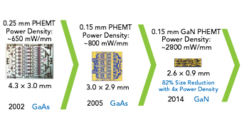
Figure 3 MMIC PA evolution from PHEMT to GaN.8
These factors and GaN’s ability to withstand a wide temperature gradient and many thermal cycles supports its suitability for mmWave applications, where intrinsic device losses are higher and heat is generated during amplification and switching. As GaN’s thermal conductivity (~1 to 3 W/cm K) is greater than the conductivity of GaAs and InP, GaN devices are inherently better at heat dissipation at high-power levels.
For the same output power, a GaN device will be a fraction of the size of GaAs and InP devices. Substantially reducing device size reduces on-chip routing and combining losses when multiple transistors are integrated on the same die. GaN’s size and power advantages are dramatic (see Figure 3).
Vertical Transistors
Typically, GaN devices have been fabricated as lateral heterojunction AlGaN/GaN HEMTs on Si or SiC substrates. Lateral GaN technologies are becoming mature and potentially reaching their voltage and power limits. At high voltage and power, lateral devices require substantially more chip area than vertical devices. Generally, vertical devices can provide higher power from a smaller area, as vertical devices withstand higher blocking voltage in the vertical direction into the bulk material.4,12 Other arguments for vertical devices are potential benefits from current spreading and thermal management.

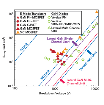
Figure 4 Ron vs. breakdown voltage of state-of-the-art vertical and lateral GaN diodes and transistors.12
Vertical GaN transistors are early in the development lifecycle. A vertical transistor technology would likely be GaN on GaN12 because GaN on GaN homoepitaxial layers have lower dislocation densities than GaN on Si or GaN on SiC. Though GaN on GaN wafers have historically been expensive, the cost has steadily declined over the last several years and larger wafer sizes are becoming available. Vertical GaN transistors have achieved breakdown voltages greater than 1 kV and current handling near 100 A.12 The evolutions of high voltage GaN transistors will likely require development of enhancement mode devices, which could be GaN trench MOSFETs or even FinFETS (see Figure 4). The figure shows the Ron and breakdown voltage performance of vertical and lateral GaN diodes and transistors, as well as the performance of 1D unipolar Si and SiC devices.
GaN & CMOS Compatibility
Significant R&D is underway to develop a GaN process that is compatible with CMOS.5,13–18 GaN epitaxy on Si substrates has rapidly developed and will enable a GaN-CMOS process in the near future. The process replaces GaN’s Au ohmic contact metal with an alternative, as Au metallization is incompatible with CMOS processes. Possible alternatives are Ti, Al, Ni or a TiN combination instead of the typical Ti/Al/Ni/Au ohmic contact metal stack.13 A TiN diffusion barrier/Schottky metal with a Cu or Al conductor layer could replace the metal gate, rather than the typical Ni Schottky gate with an Au conductor layer.14
CMOS-compatible GaN could enable GaN on Si high frequency and high-power devices to be integrated on the same IC as the digital, memory, signal processing, analog-to-digital and digital-to-analog circuits fabricated in CMOS. This capability would enable an entire transceiver containing the RF front-end, modulation, demodulation, beamforming, MIMO, signal processing and other communication or sensing features to be integrated. This could lead to pairing several GaN transceiver channels with a high performance FPGA core, enabling a single chip solution for a phased array antenna.
SUMMARY
As GaN technology brings performance and system benefits to a variety of RF applications, costs will continue to reduce, feeding an investment cycle to develop better GaN-based technologies and the development of a GaN-CMOS process. Devices capable of mmWave and sub-THz performance combined with higher power and operating voltage will open even more doors for GaN.
References
- K. Harrouche and F. Medjdoub, “GaN-based HEMTs for mm-wave Applications,” Nitride Semiconductor Technology: Power Electronics and Optoelectronic Devices, 2020, Web: hal.archives-ouvertes.fr/hal-03287288.
- “Gallium Nitride Semiconductor Devices Market Report, 2030,” Grand View Research, Web: www.grandviewresearch.com/industry-analysis/gan-gallium-nitride-semiconductor-devices-market.
- “GaN RF MARKET APPLICATIONS, PLAYERS, TECHNOLOGY, SUBSTRATES - MARKET UPDATE 2021,” Yole Développement, Web: www.yole.fr/GaN_RF_Market_Update_2021.aspx.
- “Monolithic Microwave IC Market Size - Growth Trends 2028,” Global Market Insights Inc., Web: www.gminsights.com/industry-analysis/monolithic-microwave-ic-market.
- A.-C. Liu et al., “The Evolution of Manufacturing Technology for GaN Electronic Devices,” Micromachines, Vol. 12, No. 7, Article No. 7, July 2021.
- T. M. Research, “GaN on Silicon Technology Market Growth, Trends and Forecasts | 2019 – 2027,” Digital Journal, Web: www.digitaljournal.com/pr/gan-on-silicon-technology-market-growth-trends-and-forecasts-2019-2027.
- “GaN on Silicon Technology Market,” Transparency Market Research, Web: www.transparencymarketresearch.com/gan-on-silicon-technology-market.html.
- “Heterogeneous Integration Roadmap 2021 Edition, Chapter 12: 5G Communication,” Nov. 2021, Web: eps.ieee.org/images/files/HIR_2021/ch12_5G.pdf.
- R. Chen and F. F. Wang, “SiC and GaN Devices With Cryogenic Cooling,” IEEE Open J. Power Electron, Vol. 2, 2021, pp. 315–326.
- “Qorvo Wins U.S. Government Project to Create Advanced, State-of-the-Art, RF Semiconductor Packaging Center,” Microwave Journal, Nov. 2020, Web: www.microwavejournal.com/articles/34910-qorvo-wins-us-government-project-to-create-advanced-state-of-the-art-rf-semiconductor-packaging-center.
- J. McHale, “GaN in Space, Military RF trends - Military Embedded Systems,” O. Media, June 2021, Web: dev007.militaryembedded.com/from-the-editor/gan-in-space-military-rf-trends.
- K. Hoo Teo et al., “Emerging GaN Technologies for Power, RF, Digital, and Quantum Computing Applications: Recent Advances and Prospects,” J. Appl. Phys., Vol. 130, No. 16, Oct. 2021, pp. 160902.
- X. Li, S. Gao, Q. Zhou, X. Liu, W. Hu and H. Wang, “Fabrication and Performance of Ti/Al/Ni/TiN Au-Free Ohmic Contacts for Undoped AlGaN/GaN HEMT,” IEEE Trans. Electron Devices, Vol. 67, No. 5, May 2020, pp. 1959–1964.
- T. Kawanago et al., “Advantage of TiN Schottky Gate Over Conventional Ni for Improved Electrical Characteristics in AlGaN/GaN HEMT,” 2013 Proceedings of the European Solid-State Device Research Conference (ESSDERC), Sept. 2013, pp. 107–110.
- M. Ho Kwan et al., “CMOS-Compatible GaN-on-Si Field-Effect Transistors for High Voltage Power Applications.” IEEE International Electron Devices Meeting, 2014, Web: ieeexplore.ieee.org/document/7047073.
- K. Y. Wong et al., “A Next Generation CMOS-compatible GaN-on-Si Transistors for High Efficiency Energy Systems,” IEEE Int. Electron Devices Meet, IEDM, 2015.
- L.-H. Hsu et al., “Development of GaN HEMTs Fabricated on Silicon, Silicon-on-Insulator, and Engineered Substrates and the Heterogeneous Integration,” Micromachines, Vol. 12, No. 10, Oct. 2021.
- U. Peralagu et al., “CMOS-compatible GaN-based Devices on 200mm-Si for RF Applications: Integration and Performance,” in 2019 IEEE International Electron Devices Meeting (IEDM), Dec. 2019, pp. 17.2.1-17.2.4.
