A 3D printable photopolymer resin and 3D digital light processing printing technology enable the fabrication of a high gain, V- and W-Band dielectric lens antenna prototype.
There are a slew of market forces and technology trends driving the development of wireless communication and sensing systems designed to operate in frequency bands previously only used in satellite communication, backhaul and military radar. Examples include the recently released and licensed 5G and Wi-Fi frequency bands beyond 6 GHz, the extension of V-Band allowing unlicensed use to 71 GHz and new automotive short-range radar applications from 77 to 81 GHz. With growing spectrum congestion below 6 GHz, many applications are seeking to operate in higher spectrum regimes to avoid interference.
There are also other attractive features of operation at mmWave frequencies, namely that the size of many RF electronics scale in proportion to wavelength. mmWave components and devices can often be fabricated in much smaller form factors than lower frequency components and devices (i.e., smaller antennas and other RF hardware). Examples include mmWave 5G gNodeB and antenna arrays, as well as mmWave sensing devices such as imaging systems and radar.
This is a double-edged sword, however, as the relative size of mmWave hardware shrinks, manufacturing tolerances and precision material requirements become more restrictive due to a variety of phenomena (e.g., skin effect and high RF losses). Although the promise of broad swaths of available spectrum at mmWave frequencies seems attractive, the phenomena and fabrication considerations that come into play at these frequencies are often either negligible or able to be ignored at lower frequencies.
There are some emerging technologies whose benefits cannot be realized below mmWave frequencies, such as dense active/advanced antenna arrays (AAS). Now is the dawn of mmWave technology emerging from the shadows into mainstream use, along with the accompanying design and fabrication challenges that require designers to consider new solutions.
FABRICATION CHALLENGES
Conductors are formed of metals, which can generally be reliably deposited, sputtered, formed and plated to reasonably high tolerances. They are also readily measurable. Dielectrics, however, are most often ceramics, glasses or polymers, which present nuanced production and manufacturing challenges.
The most significant electrical characteristics of conductors at mmWave frequencies are generally at the surface. This can depend on conductor thickness and the relative depth of the carrier concentration. Conductors can be plated or otherwise coated with gold or other noble metals to provide higher conductivity and a more conformal surface.
For dielectrics, which are often used to support, separate or load conductive structures, surface and bulk properties are critical and the electric field typically penetrates into, or entirely through, the dielectric material. As the electric field passes through a dielectric, some energy is absorbed (dielectric loss tangent or its reciprocal, quality factor) and converted to heat. For many dielectrics, a relatively small change in temperature can affect overall dielectric performance and dimensional stability. Consequently, dielectrics with extremely low loss tangents, less than 10-4 at 1 kHz and 10-3 at mmWave frequencies are desirable.1
Conformality of dielectric properties and dimensions of a dielectric are critical, as even small variations or gradients of a material’s dielectric performance can change the behavior of the electric field passing through it. Spatially layering or mixing of dielectric materials results in generally difficult-to-determine dielectric effects, which may result in the effective permittivity of a given dielectric structure being much different than that of the constituent dielectrics.

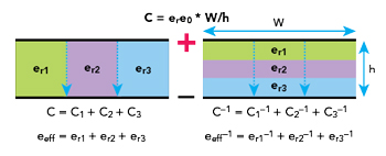
Figure 1 Parallel plate capacitor with series (left) and parallel (right) dielectric layers.
In a parallel plate capacitor, for example, the direction of the dielectric layers with respect to the capacitive plates determines the effective permittivity of the overall dielectric. For perpendicularly stacked dielectric layers, the effective permittivity is essentially additive, where parallel stacked dielectric layers (perpendicular to the electric field with equal charge) result in an effective permittivity which is the sum of the reciprocals of each layer’s dielectric constant (see Figure 1). For more complex 3D structures, this computation becomes increasingly complicated, and thus hard to analytically determine using effective medium theory.
Dielectrics for mmWave applications must be machined, deposited, developed or layered with exacting precision. The degree of precision that can be achieved is a limiting factor in determining what materials and fabrication processes are viable for a given mmWave frequency.
METASTRUCTURES
A new class of electromagnetic metastructures (e.g., metamaterials, metasurfaces, meta-atoms, metalfilms and metascreens) can be made to behave in ways that traditional dielectrics in nature, or as conformal bulk structures, cannot. Within a dielectric medium, dipole moments are induced by electric polarization of the embedded scatterers when exposed to an electric field.2 By volume averaging the dipole moments into a polarization density (P) with electric field (E), the result is an electric displacement vector (D) and permittivity (ε) as shown in Equation 1.
![]()
Although natural dielectrics and materials have only positive values for permittivity, man-made materials with special properties or structures have since been made/arranged in such a way as to yield negative refractive indexes, or negative permittivities. This is also the case for classes of magnetic metastructures that impact magnetic permeability.
The non-traditional permittivity behavior is frequency dependent, where frequencies outside the operational range of the metastructure interact with it in more traditional ways; but, within its frequency range of operation, these composite/engineered materials dramatically change the structure’s electrical performance.
Creating a gradient of refractive indices within a dielectric volume, for example, can result in behavior that physically resembles that of optical lenses, but affecting electromagnetic radiation well below that of visible light. Gradient refractive index (GRIN) structures can be designed to act as complex optical structures that yield desired radiation patterns different from that of traditional lenses with more complex and nuanced behaviors.
