

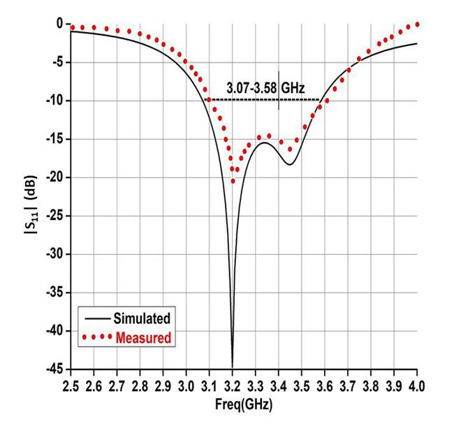
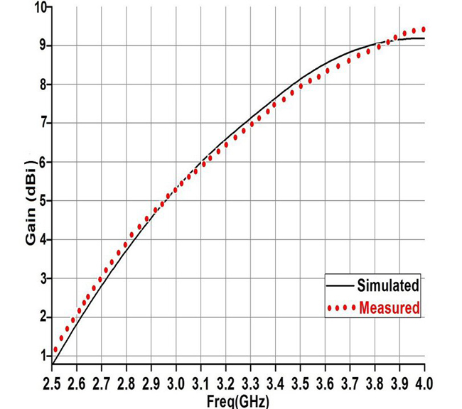
A compact circularly polarized microstrip patch antenna has an irregular hexagonal radiating patch along with two triangular coplanar parasitic patch elements of optimum size and position for WiMAX (3.3 to 3.4 GHz) applications. The two parasitic elements not only increase the resonant bandwidth but also generate circularly polarized radiation. There are no costly and difficult to fabricate slotting, slitting or other complex techniques used. The antenna has an impedance bandwidth of 510 MHz (|S11| = - 10 dB) from 3.07 to 3.58 GHz (15.34 percent) and a circular polarization bandwidth of 120 MHz (axial ratio ≤ 3 dB) from 3.29 to 3.41 GHz (3.58 percent). Its peak gain is 2.3 dB.
Circular polarization (CP) has become increasingly more popular for use in wireless communications, global navigation satellite systems and complex military systems. Linearly polarized antennas generally used in wireless mobile communication systems are prone to multipath distortion as well as polarization mismatch losses. A CP antenna reduces multipath distortion, polarization mismatch loss and transmitter/receiver orientation constraints.1,2
A CP antenna must excite two modes of equal amplitude and 90 degrees out of phase.3 This can be achieved with an antenna having two orthogonal excitation feeds.4 The two feeds, however, require two RF power sources or a power divider, which increases the the antenna’s size and complexity. A CP antenna designed with a single feed due to a modified geometry provides the benefits of a low profile and less complexity.
Many CP antennas with single feeds and modified structures have been reported in the literature using different techniques such as the introduction of slits, slots, an arrowhead-shaped slot on the radiating patch,5 stacked patches,6 and fractal defected ground structures.7 A 40.4 x 40.4 x 1.6 mm3 CP hexagonal patch antenna with elliptical and circular perturbations for better CP characteristics was designed for 2.5 GHz RFID applications.8 Another CP hexagonal microstrip antenna with the patch suspended on a coaxial feed was designed by Ray et al. for a 915 MHz GSM application.9 Shinde et al.10 described a hexagonal circularly polarized patch antenna with a 45-degree tilted narrow slot on the radiating patch and cross slots oriented at 0 and 45 degrees in the ground for WLAN. Mondal et al.11 designed a CP stacked wideband hexagonal microstrip GPS patch antenna with a diagonal-slotted patch for an intelligent transport system application. A CP hexagonal microstrip patch antenna was reported by Shinde et al. with slit, slot and stub perturbations on the radiating patch.12 The radiating patch was stacked with similar parasitic patches for the mobile satellite service band at a center frequency of 2 GHz.
In this work, a low profile circularly polarized microstrip patch antenna is designed with two optimized coplanar parasitic elements added close to the top right and bottom left side of the irregular hexagonal main radiating patch. Before adding the parasitic elements, the impedance bandwidth (|S11| = -10 dB) of the antenna is 7.3 percent. After inclusion of the parasitic elements, the impedance bandwidth increases more than two-fold to 15.34 percent. Antenna polarization also changes from linear to circular. Generally, the addition of parasitic elements is known to increase the bandwidth,13,14 but this work reports increased bandwidth as well as a change of polarization.
ANTENNA DESIGN DESCRIPTION
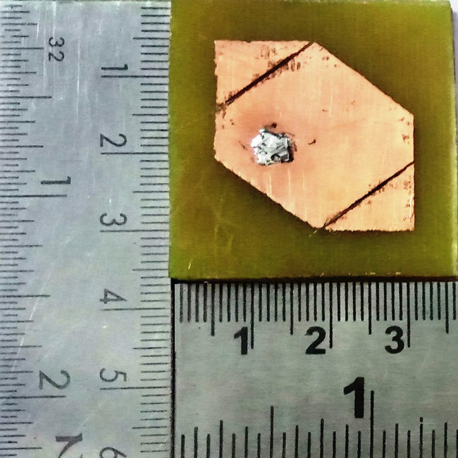
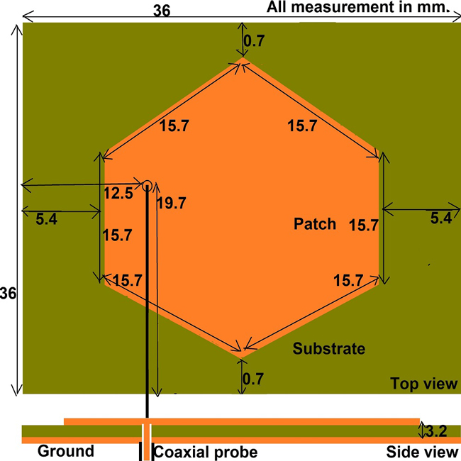
The antenna (see Figure 1) has three main parts: 1) radiating patch, 2) substrate and 3) ground plane. The radiating patch comprises an irregularly shaped hexagonal patch with 15.7, 6, 15.7, 15.7, 6 and 15.7 mm sides and two triangular coplanar parasitic elements with 14.9, 11.9, and 8.9 mm sides. The parasitic elements are located at 0.7 and 0.5 mm from the top right side and bottom left side of the irregular hexagonal patch. The 3.2 mm thick substrate is FR4 with a relative permittivity εr = 4.4 and loss tangent tan δ = 0.02. The ground plane has a 36 x 36 mm2 area. Both the radiating patch and ground plane are thin copper sheet. The total size of the antenna is 36 x 36 x 3.2 mm3. A 50 Ω coaxial probe with an SMA connector located 12.5 mm from the left edge and 19.7 mm from the bottom edge of the substrate is used for excitation.
 (1a)
(1a)
 (1b)
(1b)
 (1c)
(1c)Fig. 1 Circularly polarized patch antenna design (a), top (b) and bottom (c) views of the fabricated antenna.
DESIGN PROCEDURE
Many microstrip patch antennas have been designed, developed and reported with a regularly shaped radiating patch, such as square, rectangular, triangular and circular. An investigation of a microstrip patch antenna with a hexagonal radiating patch, however, has shown better efficiency as compared to these other geometries.15 Consequently, the hexagonal shaped radiating patch is selected for this application.
The regularly shaped hexagonal patch antenna and circular patch antenna are closely; consequently, the resonant frequency of a circular patch antenna, as described by Equations (1), (2) and (3) is used to calculate the primary resonant frequency of the regularly shaped hexagonal patch antenna.16

(1)

(2)
where
fr=Resonant frequency of the circular patch antenna.
Xmn = 1:8411 for mode TM11.
c=Velocity of light in free space.
ɛr=Relative permittivity of the substrate.
ae=Effective radius of the circular patch.
h= Height of the substrate
and

(3)
where s is the side length of the regular hexagonal patch.
After determining 2.93 GHz as the primary resonant frequency of the microstrip antenna with a regularly shaped hexagonal radiating patch having 15.7 mm sides, HFSS software is used for initial design and simulation. The simulation provides a primary resonant frequency band from 2.8 to 3 GHz) for (|S11| ≤ −10 dB) for a 200 MHz bandwidth at a probe position 12.5 mm from left edge and 19.7 mm from bottom edge of the substrate (see Figure 2a, b).
 (2a)
(2a)
 (2b)
(2b)
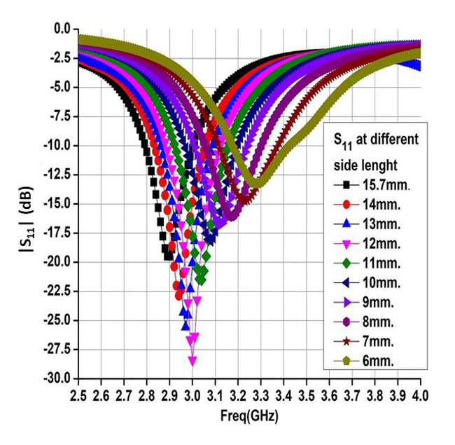
The operating frequency band of the initial antenna design is lower than the desired WiMAX band of 3.3 to 3.4 GHz. The frequency band shifts with the variation of the surface current path length caused by a modification of the antenna. It shifts toward the lower side of the frequency range when the surface current path length increases and toward the higher side of the frequency range when surface current path length decreases.
To shift the resonant frequency band higher, the length of the left and right sides of the regular hexagonal patch are reduced by 1 mm at a time continuously with the same probe position and subsequent results are observed. Due to the reduction of the side lengths, the effective resonant length of the patch decreases and the current path length is reduced. This shifts the resonant frequency band higher (see Figure 2c). At 6 mm for both sides of the hexagonal patch, the antenna operating band is 3.18 to 3.42 GHz with an impedance bandwidth of 7.3 percent for (|S11| ≤ −10 dB), which covers the WiMAX band.
 (2c)
(2c)
After making the above modifying the initial design, the regular hexagonal patch becomes an irregular hexagon with side lengths of 15.7, 6, 15.7, 15.7, 6 and 15.7 mm (see Figure 2d). This structure can be used as a linearly polarized antenna for the WiMAX band, but it suffers from polarization mismatch losses and multipath distortion. To change the polarization of the antenna from linear to circular while enhancing the impedance bandwidth, two triangular coplanar parasitic elements are incorporated near the top right side and bottom left side of the irregular hexagonal radiating patch (see Figure 1a).
 (2d)Fig. 2 Regular hexagonal patch antenna design (a), |S11| (b), |S11| with different side dimensions (c) and irregular hexagonal patch antenna design (d).
EFFECT OF PARASITIC ELEMENTS
The parasitic elements excite different resonant modes close to the primary resonant mode generated by the main radiating patch. This is due to mutual coupling between the radiating patch and the parasitic elements through their associated fringing electromagnetic fields and leads to a wider bandwidth.13, 14
After incorporation of the two triangular parasitic elements, a parametric optimizaion of element position and dimensions is done using HFSS, observing |S11|, axial ratio and input impedance (see Figure 3). Triangular parasitic elements with dimensions 14.9 x 11.9 x 8.9 mm spaced 0.7 and 0.5 mm from the top right side and bottom left side of the irregular hexagonal are determined to be optimum.
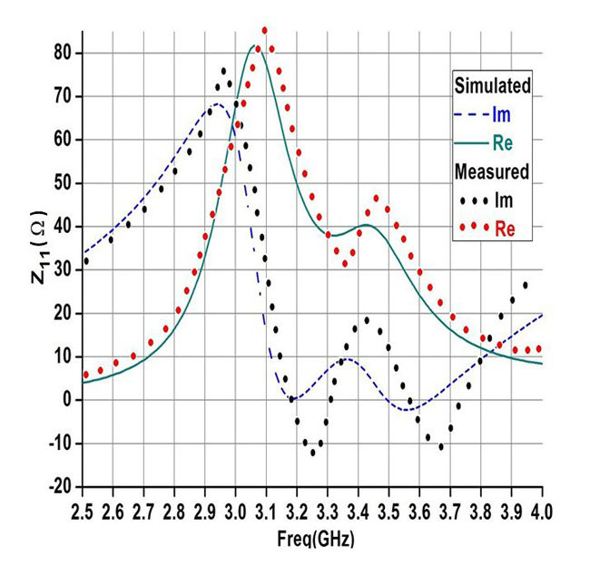
Without parasitic elements, the resonant bandwidth is 7.3 percent. The impedance bandwidth is 15.34 percent, more than doubled, with the addition of the elements, as shown in Figure 3a. The parasitic elements also reduce the antenna input impedance (see Figure 3b), which improves the impedance match.
 (3a)
(3a)  (3b)
(3b)
 (3c)
(3c)Fig. 3 |S11| (a), Z11 (b) and axial ratio (c) before and after adding the parasitic elements. Phase difference after adding the parasitic elements (d).
Before the addition of parasitic elements, the modified antenna shown in Figure 2d is linearly polarized, which is evident from the high axial ratio in Figure 3c. After the addition of the parasites elements, the current distribution is altered such that the antenna generates two orthogonal degenerate modes (TM01 and TM10) with the same magnitude. The phase difference between them, however, is not equal to 90 degrees, which is required for CP.
To meet the requirement for orthogonality, the size of the parasitic elements is optimized so that the effective surface current path associated with TM01 mode is slightly greater in one direction, as compared to TM10 mode in another direction. This makes the TM10 mode resonant frequency slightly higher than that of the TM01 mode resonant frequency so that the phase difference between them is 90 degrees.
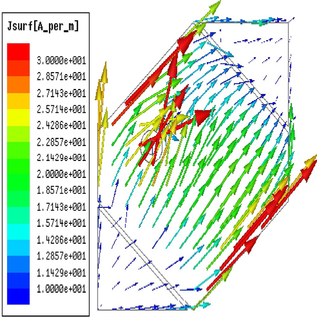
By selecting proper dimensions and locations of the parasitic elements, the conditions required for CP are satisfied.17-20 Axial ratio and phase difference are measures of CP. If the axial ratio is less than 3 dB and the phase difference is around 90 degrees over a frequency range, then the antenna is considered circularly polarized within that range. The antenna axial ratio and phase difference (see Figures 3c and d), verify its CP in the desired band. The current distributions of the antenna at 3.35 GHz and at different instants of time are shown in Figure 4.
 (4a)
(4a)
 (4b)
(4b)
 (4c)
(4c)
 (4d)
(4d)Fig. 4 Simulated surface current distribution at 3.35 GHz for q = 0 (a), 90 (b), 180 (c) and 270 (d) degrees.
EQUIVALENT CIRCUIT MODEL
The equivalent circuit model shown in Figure 5 represents the operation of the antenna in Figure 1. The driven hexagonal patch is modeled with two parallel resonators in series. The parasitic triangular patches are modeled as two different RLC resonators coupled to the driven patch through a transformer type mutual coupling mechanism. A comparison of |S11| from the equivalent circuit model with the HFSS simulation shows excellent correlation.
 (5a)
(5a)
 (5b)
(5b)Fig. 5 Antenna equivalent circuit model (a) and comparison of resulting |S11| with HFSS (b).
MEASUREMENT RESULTS
Measurements of |S11|, radiation patterns, axial ratio, input impedance, gain and radiation efficiency are made on the prototype antenna in Figure 1 using a Keysight E5071B VNA in an anechoic chamber. Simulated and measured results are shown in Table 1.
Table 1
Simulated and measured results
Parameters |
Simulated |
Measured |
Resonant Band: |S11| ≤ −10 dB |
3.07 to 3.58 GHz |
3.1 to 3.61 GHz |
Impedance Bandwidth: |S11| ≤ −10 dB |
510 MHz, 15.34% |
510 MHz, 15.2% |
CP Resonant Band: AR ≤3 dB |
3.29 to 3.41 GHz |
3.3 to 3.4 GHz |
CP Bandwidth: AR ≤3 dB |
120 MHz, 3.58% |
100 MHz, 2.99% |
Peak Gain (dB) |
2.3 at 3.35 GHz |
2 at 3.35 GHz |
Application |
WiMAX (3.3 to 3.4) GHz |
|
Simulated and measured results closely match with slight differences (see Figure 6). Discrepancies are attributed to fabrication errors, irregular soldering of connector, an imperfect environment21,22 and uncertainties in substrate relative permittivity.23 Figures 6c and d show right-hand CP and left-hand CP radiation patterns in the E-plane (X-Z) and H-plane (Y-Z) at 3.35 GHz with good agreement of simulation with measurement.
 (6a)
(6a)
 (6b)
(6b)
 (6c)
(6c)
 (6d)
(6d)
 (6e)
(6e)
 (6f)
(6f)
 (6g)
(6g)Fig. 6 Measured and simulated S11 (a), axial ratio (b), X-Z plane normalized radiation pattern at 3.35 GHz (c), Y-Z plane normalized radiation pattern at 3.35 GHz (d), gain (e), input impedance (f) and radiation efficiency (g).
A comparison with similar type antennas in the literature is summarized in Table 2.
Table 2
COMPARISON WITH SIMILAR WORK
(λ0 is the free space wavelength)
Ref. No. |
Antenna size (λ0 x λ0 x λ0) with Side Length of Hexagonal Patch (mm) |
Operating Frequency (GHz) |
Impedance Bandwidth |S11| ≤ −10 dB (MHz, %)
|
Axial Ratio Bandwidth AR ≤ 3 dB (MHz, %) |
Gain (dBi) |
8 |
(0.33 × 0.33 x 0.01) 17.52 |
2.45 |
100, 4.08
|
143, 5.8
|
4.5 |
9 |
----- 92.4 |
0.915 |
70, 7.65 |
16.2, 1.77 |
9.2 |
10 |
(0.5 x 0.5 x 0.03) 8.17 |
5 |
300, 6.25
|
-----, -----
|
4.8 |
12 |
(0.4 x 0.4x 0.01) 20 |
2 |
0.052, 2.58 |
34.2, 1.71 |
0.16 |
15 |
(0.6 x 0.6 x 0.04) 11 |
3.6 |
230, 6.35
|
120, 3.33
|
6.6 |
24 |
----- 51 mm |
0.915 |
26.2, 2.86 |
6.01, 0.66 |
----- |
25 |
(0.22 x 0.19 x 0.04) At 3.5 GHz 14 |
3.5 and 5.18 |
120, 3.43 and 250, 4.83 |
24, 0.69 and 53, 1.02 |
3.8 and 5.4 |
26 |
(0.48 × 48 x 0.01) 20 |
2.39 |
203, 8.49 |
42.6, 1.8 |
7.9 |
27 |
(0.67 x 0.67 x 0.02) 11 |
4 |
340, 8.5
|
90, 2.25
|
6.5 |
|
This Work |
(0.42 x 0.42 x 0.04) (15.7, 6,15.7, 15.7, 6, 15.7) |
3.35 |
510, 15.34
|
120, 3.58
|
2.3 |
CONCLUSION
A low profile circularly polarized microstrip antenna has a hexagonal radiating patch with two optimized parasitic elements. The parasitic elements increase the resonant bandwidth as well as providing CP without additional complexity. The antenna is low profile, simple in structure, low-cost and easy to fabricate. It generates linear polarization without parasitic elements and CP with parasitic elements for the WiMAX frequency band (3.3 to 3.4 GHz).
References
- Y. Sung, “Circularly Polarized Patch Antenna with Two Different C-Shaped Ring Structures,” Microwave and Optical Technology Letters, Vol. 61, No. 12, December 2019, pp. 2773-2780.
- K. Li, F. -W. Wang, Y. -H. Ren and Y. -M. Cai, “Dual Band Circularly Polarized Antenna with Harmonic Suppression Performance,” International Journal of RF and Microwave Computer-Aided Engineering, Vol. 29, No. 8, August 2019.
- V. Sharma and M. M. Sharma, “Dual Band Circularly Polarized Modified Rectangular Patch Antenna for Wireless Communication,” Radioengineering, Vol. 23, No. 1, April 2014, pp. 195-202.
- Y. -X. Guo, L. Bian L and X. Q. Shi, “Broadband Circularly Polarized Annular-Ring Microstrip Antenna,” IEEE Transactions on Antennas and Propagation, Vol. 57, No. 8, August 2009, pp. 2474-2477.
- A. K. Gautam, A. Kunwar and B. K. Kanaujia, “Circularly Polarized Arrowhead-Shape Slotted Microstrip Antenna,” IEEE Antennas and Wireless Propagation Letters, Vol. 13, March 2014, pp. 471-474.
- S. I. Latif and L. Shafai, “Circular Polarization from Dual-Layer Square-Ring Microstrip Antennas,” IET Microwaves Antennas & Propagation, Vol. 6, No. 1, January 2012, pp. 1-9.
- K. Wei, J. Y. Li, L. Wang, R. Xu and Z. J. Xing, “A New Technique to Design Circularly Polarized Microstrip Antenna by Fractal Defected Ground Structure,” IEEE Transactions on Antennas and Propagation, Vol. 65, No. 7, July 2017, pp. 3721-3725.
- K. C. Prakash, P. V. Vinesh, M. P. Jayakrishnan, R. Dinesh, A. Mohammad and K. Vasudevan, “Hexagonal Circularly Polarized Patch Antenna for RFID Applications,” International Journal on Cybernetics & Informatics, Vol. 5, No. 2, April 2016, pp. 173-182.
- K. P. Ray, D. M. Suple and N. Kant “Suspended Hexagonal Microstrip Antennas for Circular Polarization,” International Journal of Microwave and Optical Technology, Vol. 5, No. 3, May 2010, pp. 119-123.
- M. Saravanan and M. J. S. Rangachar, “Design of Wide Beam Hexagonal Shaped Circularly Polarized Patch Antenna for WLAN Application,” 8th International Conference on Soft Computing and Pattern Recognition, January 2018.
- T. Mondal, S. Samanta, R. Ghatak and S. R. B. Chaudhuri, “A Novel Hexagonal Wideband Circularly Polarized Stacked Patch Microstrip Antenna,” Microwave and Optical Technology Letters, Vol. 57, No. 11, November 2015, pp. 2548-2554.
- J. P. Shinde, RajKumar and M. D. Uplane, “Circular Polarization in Stacked Hexagonal Shaped Microstrip Antennas,” International Journal of Advanced Research in Electrical, Electronics and Instrumentation Engineering, Vol. 2, No. 7, July 2013, pp. 3376-3384.
- H. -X. Lu, F. Liu, M. Su and Y. -A. Liu, “Design and Analysis of Wideband U-Slot Patch Antenna with U-Shaped Parasitic Elements,” International Journal of RF and Microwave Computer-Aided Engineering, Vol. 28, No. 4, November 2017.
- G. Kamalaveni and M. M. Ganesh, “A Compact Parasitic Ring Antenna for ISM Band Applications,” Frequenz, Vol. 70, November 2016, pp. 513-519.
- A. O. Fadamiro, J. D. Ntawangaheza, O. J. Famoriji, Z. Zhang and F. Lin, “Design of a Multiband Hexagonal Patch Antenna for Wireless Communication Systems,” IETE Journal of Research, October 2019.
- C. A. Balanis, Antenna Theory (Analysis and Design), Wiley publication, 4th edition, New Jersey, U.S., 2016.
- S. Kumar, R. K. Viswakarma, R. Kumar, J. Anguera and A. Andujara, “Slotted Circularly Polarized Microstrip Antenna for RFID Application,” Radioengineering, Vol. 16, No. 4, December 2017, pp. 1025-1032.
- Y. Sung, “Axial Ratio-Tuned Circularly Polarized Square Patch Antenna with Long Stubs,” International Journal of Antennas and Propagation, Vol. 2018, November 2018.
- K. Saraswat, T. Kumar and A. R. Harish, “A Corrugated G-Shaped Grounded Ring Slot Antenna for Wideband Circular Polarization,” International Journal of Microwave and Wireless Technologies, Vol. 12, No. 5, June 2020, pp. 431-436.
- K. Ding, C. Gao, D. Qu and Q. Yin, “Compact Broadband Circularly Polarized Antenna with Parasitic Patches,” IEEE Transactions on Antennas and Propagation, Vol. 65, No. 9, September 2017, pp. 4854-4857.
- S. Kumar, K. W. Kim, H. C. Choi, S. Saxena, R. Tiwari, M. K. Khandelwal and B. K. Kanaujia, “A Low Profile Circularly Polarized UWB Antenna with Integrated GSM Band for Wireless Communication,” International Journal of Electronics and Communications, Vol. 93, September 2018, pp. 224-232.
- N. Sharma and S. S. Bhatia SS, “Split Ring Resonator Based Multiband Hybrid Fractal Antennas for Wireless Applications,” International Journal of Electronics and Communications, Vol. 93, September 2018, pp. 39-52.
- B. Yang, M. Chen and L. Li, “Design of a Four-Element WLAN/LTE/UWB MIMO Antenna Using Half-Slot Structure,” International Journal of Electronics and Communications, Vol. 93, September 2018, pp. 354-359.
- K. P. Ray, D. M. Suple and N. Kant, “Perturbed Hexagonal Microstrip Antenna for Circular Polarization,” Applied Electromagnetics Conference, December 2009.
- K. Qian and X. Tang, “Compact LTCC Dual-Band Circularly Polarized Perturbed Hexagonal Microstrip Antenna,” IEEE Antennas and Wireless Propagation Letters, Vol. 10, October 2011, pp. 1212-1215.
- J. P. Shinde, R. Kumar and M. D. Uplane, “Circular Polarization in Defected Hexagonal Shaped Microstrip Antenna,” Wireless Personal Communications, Vol. 75, No. 2, March 2014, pp. 843-856.
- U. K. Sain and P. K. Gupat, “Bandwidth Enhancement of Circularly Polarized Hexagonal Microstrip Patch Antenna using L-Cut in Patch,” International Journal of Current Engineering and Technology, Vol. 6, No. 1, February 2016, pp. 251-254.