The satisfaction that mobile phones can provide is highly dependent on their autonomy. Three factors can be easily identified which have a strong influence on autonomy: the power consumption of the mobile phone, the intensity of the electromagnetic field near the mobile and the battery capacity. The first of these factors is addressed and low consumption architecture for mobile phones is presented in this article.
During the past five years, the algorithms used to manage power resources have been improved. At the same time, the power supply to the main circuits has decreased from 7 to 3 V for the same current. Mobile battery packs were also improved.1 Currently, mobiles have an autonomy of about one week in the standby mode versus three days in 1995 and approximately five hours in the communication mode versus two hours in 1995.
A mobile phone has rather high power consumption when in the communication mode. Much research is being conducted to improve the efficiency of the radio frequency power amplifier. New transistors on recently developed substrates, combined with new amplifier designs, give promising results for the future.1 However, most of the time the power amplifier is in an idle mode. In this case, only the receiver draws power from the battery. Therefore, a significant reduction of power consumption in the receiver produces a strong increase of the autonomy of the mobile itself.
In a radio frequency receiver, the first stage shifts the modulated high frequency signal to a lower one. The second stage controls the digital demodulation of the baseband signal produced by the first stage. The reduction in power consumption of the digital stage follows the general reduction of digital circuits. The analog stage requires a more specific effort to reduce its power consumption. Today, the autonomy observed in mobile phones shows a consumption of 200 to 250 mW for the analog part of the receiver (if active five percent of the time). In the last five years, the challenge was to develop a radio frequency front-end design that was simultaneously usable in two bands - 900 MHz and 1.8 GHz. All the circuits developed are integrated circuits for heterodyne or superheterodyne receivers.2,3 Some recent studies have tested new technologies, such as silicon BiCMOS technology4 or unused receiver designs, but have always been based on integrated circuits.5 Changing the receiver structure as well as its circuit has been chosen to improve mobile phone autonomy.
To reduce the power consumption, the currents and voltages supplied to all the various circuits must be as low as possible. The characteristics of each active component and the links between the various receiver circuits must be optimized. This is made possible by developing microwave monolithic integrated circuits or by designing hybrid circuits. To quickly develop a prototype of a low cost receiver with very low consumption, the second solution was used. Indeed, this solution gives complete freedom in the design of the circuit and in the choice of the active components, and makes it possible to evaluate, in real situations, the performance of the chosen solution. Due to the high frequency of the signal to be received (1.89 GHz), it is possible to develop particular designs of hybrid circuits with microstrip elements in place of lumped components for mixers, amplifiers, etc.
Although the concept of such combined applications of hybrid structures and microstrips is difficult, their implementation in real circuits and their manufacture is quite easy. One drawback of such an approach is the relatively large dimension of the resulting receiver. This approach has been implemented by developing a receiver operating on the DCS 1800 standard6 for mobile telecommunications that has a specific architecture. In order to validate the design, a prototype was built using an epoxy substrate in spite of the fact that such a substrate is not optimized to reduce the dimensions of the receiver.
Choice of Receiver Design
The modulation used in a DCS 1800 compatible receiver is a gaussian minimum shift keying (GMSK) modulation, and the sensitivity required by this standard6 implies a very efficient technique of demodulation. The GMSK modulation comes from the minimum shift keying modulation (MSK).
GMSK Modulation
The bit di  [0,1] to be transmitted is encoded using first a differential code and then a transition code. The new information
  i
i  [-1,1] is transposed as a continuous variation of the phase of the carrier. To obtain the GMSK modulation, the
  i data are filtered. The Gaussian filter improves the spectral efficiency, but it creates inter-symbol interferences (ISI) that do not exist with the MSK modulation.7
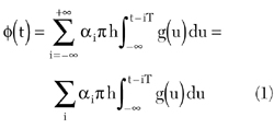
According to DCS 1800 standard,6 the phase of the carrier is defined by Equation 1:

In Equation 1,

is the modulation factor. The elementary frequency variation g(t) results from a convolution between the rectangle function rect(t) that defines the digital pattern and the unit pulse response of the Gaussian filter h(t)

The DCS 1800 standard defines:

and

with

The variation of the phase during a bit time is

Due to the similitude of the pattern-averaged phase transition trajectory between the MSK modulation and the GMSK modulation, it is reasonable to use MSK results to estimate the bit error rate (BER) of the GMSK modulation.9
Assuming that similitude, the GMSK modulation can be demodulated as a two staggered quadrature modulated binary phase shift keying (PSK) signal,7,8,9 or as a differential phase modulation (DPSK),8,10 or as a frequency modulation.8 Results in the literature make it possible to classify the demodulation techniques according to their BER (Figure 1 ). The coherent demodulation with an I/Q demodulator is the best demodulation. For this reason, the present work has been carried out with such a demodulation for the DCS 1800 standard.

Zero-IF Approach
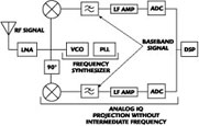
Three types of circuit can be considered for the I/Q demodulator11: a superheterodyne receiver with a digital separation of the I and Q signals, a superheterodyne receiver with two analog outputs for the I and Q signals, and a zero-IF receiver with two analog outputs for the I and Q signals. These receivers use one or two frequency translations to shift the modulated high frequency signal received at the antenna to a lower frequency compatible with the circuitry used for the demodulation and digital processing. For the three architectures, the different circuit blocks are defined as:
LNA = low noise amplifier
VCO = voltage-controlled oscillator
PLL = phase lock loop
IF filter = intermediate frequency filter
LF AMP = low frequency amplifier for baseband signal
LOG AMP = logarithmic low frequency amplifier
ADC = analog-to-digital converter
DSP = digital signal processor
LO = local oscillator

A receiver, with a superheterodyne structure (see Figure 2 ), uses a precise under sampling frequency in order to keep the I and Q samples within one output. The need to use such a particular sampling frequency introduces high constraints in the design. Since this frequency must be relatively high, it leads to a high electrical consumption. Moreover, the superheterodyne structure of the receiver implies two frequency translations, with two mixers, some intermediate frequency amplifiers and filters. All these circuits increase the power consumption of the receiver. For these reasons, this architecture is not the most efficient in terms of power consumption.

The second possible architecture shown in Figure 3 is also based on a superheterodyne design, but only uses one intermediate frequency. After the first mixer, the modulated signal is separated into two channels. On each one, a second frequency translation shifts directly the modulated signal from the intermediate frequency to the baseband. Such a receiver has two analog outputs to provide the I and Q signals, and the sampling frequency can be as low as possible according to the baseband signal. This decreases the power consumption. But as a double superheterodyne receiver, it requires many circuits at the intermediate frequency. Moreover, due to the zero intermediate frequency, it is difficult to filter the image frequency and noise that comes from radio frequency adjacent channels. Because of the first frequency translation, this architecture is not completely optimized towards the goal of power consumption reduction.

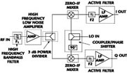
The third possible structure is a double zero-IF receiver (Figure 4 ). After a first amplification by a low noise amplifier, the modulated signal is separated into two channels with a single frequency translation on each one. The modulated signal is shifted from the high frequency (1.8 GHz) to the baseband. This structure uses a sampling frequency that can be as low as possible according to the baseband signal. The single frequency translation limits the number of circuits needed to achieve the demodulation. There is no intermediate filter and only two mixers. This suppresses some losses but requires stronger filtering in order to reduce the noise from radio frequency adjacent channels. Nevertheless, this structure is optimized to reduce the power consumption.5 For these reasons, this architecture has been chosen to develop the receiver.

Experimental Results
Using microstrip lines, various active circuits were replaced by passive ones. As an example, the power divider and phase shifter used to provide the two I and Q channels are combined in a single element in the VCO input. The two functions are implemented using a branch-line directional coupler11,13 with very good performance: -20 dB isolation and -3 dB transmission losses for each output, -20 dB impedance matching for each port and 91° phase shift from 1805 to 1880 MHz between the two outputs.
Figure 5 is a detailed block diagram of the receiver that was developed using hybrid technology, except for the frequency synthesizer. That specific part of the circuit is on another board using the same technology for the design of the VCO but the PLL used is a classic commercial circuit.12

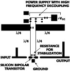
Microstrip lines are also used to realize the impedance matching11 for each active block, with good accuracy and reproducibility. Figure 6 shows how the low noise amplification is achieved in this way by three identical stages. Each low noise amplifier uses a low noise, high gain, high frequency, silicon bipolar transistor in a common emitter design (Figure 7 ). To achieve good 50 W matching simultaneously at the input and output of the amplifier, a gain limitation is introduced, using a resistance between the collector and base. This feedback gain control suppresses completely the natural instability of the common emitter design. The consumption of each low noise amplifier is 2 mA at 3 V for 9 dB gain over the 1805 to 1880 MHz band with a noise factor of 2 dB. The RF amplification is critical in a zero-IF frequency receiver because of the lack of amplification at an intermediate frequency.
Another critical active circuit is the zero-IF mixer. The presence of a high frequency (1.8 GHz) signal at the two inputs and a low frequency (300 kHz) signal at the output requires some care in the design. In these two frequency ranges, the active component, a silicon bipolar transistor, has different behavior. Thus the design must integrate such double characteristics, especially in connection to the other circuits of the receiver. To minimize the power consumption, a mixer has been designed using only one transistor, operating as a linear amplifier with its gain modulated by the local oscillator signal applied to the emitter. In such a way, intermodulation is also reduced. The baseband signal present at the emitter makes it necessary to use a high frequency bandpass filter for decoupling the mixer from the other high frequency modules. Figure 8 shows the implemented mixer, after simulation, which incorporates a very small number of components. It insures a 5 dB gain for a consumption of 0.5 mA at 3 V with a low noise factor typically of the order of 5 dB. Using the same approach, all the various functions of the receiver have been developed.11

The last RF stages of the receiver are active low pass filters with an AC coupling for the I and Q outputs. The AC coupling is possible because of the GMSK modulation used. This AC coupling suppresses the effect of the received RF power on the DC level.
Receiver Validation
The tests of the complete prototype were carried out using a very accurate frequency generator modulated by an internal IQ modulator. Signals on I and Q channels are given by arbitrary waveform generators. The sequence used is cyclic and the elementary frame is 16 bits long (0010011101101011). The demodulated signals on channels I and Q are recorded on a digital oscilloscope. A post-processing is made on a computer. To validate the efficiency of this receiver, the corresponding frequency modulation signals have been calculated. This measured data are compared to the calculated results (Figure 9 ) using the mathematical definition of GMSK modulation in the DCS 1800 standard. Such a comparison is necessary to verify that the I and Q signals are well demodulated without distortion due to an eventual malfunction of the electronics. A measurement of BER is not sufficient to validate the analog part of the zero-IF receiver.

Zero-IF Architecture Validation
It is first necessary to check that the zero-IF architecture correctly demodulates the signal. When plotting I versus Q, one expects a circle. In Figure 10 , the experimental data show the expected behavior. Channels I and Q are well balanced and properly in quadrature. The post-treatment on the recorded values of I and Q (Figure 11 ) shows that the frequency variation is the same as that of the test signal. The chosen architecture operates properly. The balance and accuracy of the phase shift is due to the design of the circuit and to the use of passive components. That result is achieved for the complete reception band (1805 to 1880 MHz).
It is then possible to check that the receiver operates in agreement with the DCS 1800 standard specifications.6 Table 1 presents the measurements carried out on the prototype for frequencies ranging from 1805 to 1880 MHz, compared to the values imposed by the DCS 1800 standard at the center frequency of the receiving band. The power indicated is the power level of the signal or the interferer for which a BER of 10-5 has been measured.

As can be seen, the selectivity is good. Concerning the saturation, the measurements were carried out without gain control at the input amplifiers. Under such unfavorable conditions, both the saturation and intermodulation are very close to the specifications. Some minor adjustments are needed. By properly choosing the biasing point and gain of the amplifiers, it is quite easy to fall within the required range.
It can be seen that during the measurements, the local synthesizer uses the reference clock of the generator as the reference for the PLL. There is no carrier leakage. Some tests with artificial carrier leakage up to 1 kHz seem to give a 3 dB decrease of the sensitivity. However, as observed on commercially marketed GSM receivers, carrier synchronization gives results better than 10 Hz with a continuous control of the reference clock of the circuit. Carrier leakage does not seem to be a critical blocking point of the zero-IF architecture used.
In conclusion, the chosen structure leads to a receiver that operates properly and satisfies the DCS 1800 standard.

Power Receiver Consumption
The described prototype requires a 30 mW power supply at 3 V.11 However, a full receiver also includes a frequency synthesizer. The synthesizer12 that was developed has a consumption of 44 mW at 3 V (11 mW for the VCO and 33 mW for the commercial PLL). The power consumption of the full receiver is 74 mW at 3 V. For comparison, the power consumption of commercially available receivers is of the order of 210 mW at 3 V including 54 mW for the synthesizer.14 Other prototypes of direct-conversion architectures, without hybrid circuits, show a power consumption reduction of the radio frequency receiver of only 10 to 20 mW.5

When the receiver is active, the reduction in power consumption achieved in this work is close to 135 mW, or 60 percent of the typical power consumption. Further improvements are still possible, for example, by choosing newer generations of PLLs for the frequency synthesizer and new transistors for active components. Of course, with daily use of a mobile phone, the reduction of the power consumption in the idle mode is less than 60 percent due to the contributions of the other parts of the equipment. The reduction also depends on the quality of the radio-telecommunication network and on the mobile phone software.
|
Table 1 | |||
|
Contraint |
Frequency |
Measured |
Required |
|
Sensitivity |
1.8426 GHz |
-102 |
-100 |
|
Selectivity | |||
|
Useful signal |
f0=1.8426 GHz |
-85 |
-85 |
|
Modulated interferer on the co-channel |
f=1.8426 GHz |
-90 |
-94 |
|
On the adjacent channels |
f=f0±200 kHz |
-72 |
-76 |
|
Saturation (Blocking) | |||
|
Useful signal |
f0=1.8426 GHz |
-97 |
-97 |
|
In the RF band |
f=f0+600 kHz |
-37 |
-43 |
|
1785 < f < 1920 |
f=f0-600 kHz |
-37 |
-43 |
|
Modulated interferer |
f=f0+1.2 MHz |
-32 |
-43 |
|
Out of the RF band |
100 kHz < f < 1705 MHz |
-4 |
0 |
|
Nonmodulated interferer |
1920 MHz < f < 1980 MHz |
-10 |
-12 |
|
Intermodulation | |||
|
Useful signal |
f0=1.8426 GHz |
-97 |
-97 |
|
f1 nonmodulated interferer |
f1=1.8434 GHz |
-50 |
-49 |
|
f2 modulated interferer |
f2=1.8442 GHz |
-50 |
-49 |
Conclusion
The present study was aimed at ways to reduce the power consumption of a mobile phone. It has been shown that by choosing a zero-IF structure, it is possible to drastically reduce the power consumption of the receiver. A prototype was built using hybrid circuits and microstrip components. A reduction of power of 60 percent, as compared to currently available receivers, was achieved while fully satisfying the DCS 1800 standard.
The same architecture can be used in other telecommunication standards, leading to commercially feasible products. For instance, it has already been implemented in DECT phones, operating around 1889 MHz, now being manufactured in millions of units per year. Moreover, by replacing the epoxy substrate by a proper dielectric, the size of the microstrip components can be easily reduced.
References
1. P. Asbeck, J. Mink, T. Itoh and G. Haddad, "Device and Circuit Approaches for Next Generation Wireless Communications," Microwave Journal , Vol. 42, No. 2, February 1999.
2. R.G. Meyer and W.D. Mack, "A 1 GHz BiCMOS RF Front-end IC," IEEE Journal of Solid-State Circuits , Vol. 29, No. 3, March 1994, p. 350.
3. Motorola Product Division, "A 1.9 GHz Chipset for PCS Applications," Microwave Journal , Vol. 38, No. 6, June 1995, pp. 96-100.
4. COMMQUEST (an IBM company) "SIGe Front-end RFICs," Microwave Journal , Vol. 41, No. 12, December 1998, pp. 114-116.
5. C.D. Hull, J.L. Tham and R.R. Chu "A Direct-conversion Receiver for 900 MHz (ISM Band) Spread-spectrum Digital Cordless Telephones," IEEE Journal of Solid-State Circuits , Vol. 31, No. 12, December 1996, p. 1955.
6. E.T.S.I., "European Digital Cellular Telecommunication System GSM-DCS (phase 2)," September 1994.
7. J.C. Bic, D. Duponteil and J.C. Imbeaux, Eléments de Communications Numériques , Tome 1, Dunod, Paris, France, 1986.
8. J.G. Proakis, Digital Communications , McGraw-Hill Inc., International Editions, Third Edition, Singapore, 1995.
9. K. Murota and K. Hirade, "GMSK Modulation for Digital Mobile Radio Telephony," IEEE Transactions on Communications , Vol. COM-29, No. 7, July 1981, pp. 1044-1050.
10. J.C. Bic, D. Duponteil and J.C. Imbeaux, Eléments de Communications Numériques , Tome 2, Dunod, Paris, France, 1986.
11. E. Géron, "Etude et Réalisation d'un Récepteur Radiofréquence Basse Consommation Compatible DCS 1800," Thése de Doctorat de l'Université Pierre et Marie CURIE (Paris 6), Paris, France, January 1997.
12. P. Geng, "Etude et Réalisation d'un Synthétiseur de Fréquence Basse Consommation pour Radiotéléphone Mobile," Thése de Doctorat de l'Université Pierre et Marie CURIE (Paris 6), Paris, France, October 1996.
13. R.E. Collin, Foundation for Microwave Engineering , McGraw-Hill Inc., International Editions, Singapore, 1992.
14. Philips, "Semiconductors for Wireless Communications," Data Handbook IC17 (a and b), 1998.
 Emmanuel Géron graduated from Ecole Supérieure de Physique et de Chimie Industrielle (E.S.P.C.I.) of the City of Paris in 1992, and obtained his PhD degree in electronics from the University of Paris in 1997. He has been an assistant professor at E.S.P.C.I. since 1997.
 Jacques Lewiner obtained his PhD degree in physics from the University of Paris in 1969. He has been a professor at Ecole Supérieure de Physique et de Chimie Industrielle (E.S.P.C.I.) of the City of Paris since 1973.
