A number of factors are driving the design of high speed digital packaging. At the assembly level, metal boxes are the dominant configuration due to mounting and interconnect constraints. The next assembly connectivity is accomplished through cables, requiring coaxial connectors. Since a variety of companies manufacture many of the functions, each device utilizes different housings and connectors. At the chip level, the device mounting is made with a ball grid array (BGA) on a carrier or assembled in a joint electron device engineering council (JEDEC) style package. But with the operating frequencies of digital assemblies increasing into the microwave domain, the package requirements are changing.
Design Drivers

Electrical performance is key. The electrical interconnects have to be designed for the correct impedance and have low transmission losses. As the digital speeds continue to increase and enter the microwave and millimeter-wave frequency domain, the components are no longer lumped, but are now distributed and thus require transmission line design. Wire bonds, gaps between substrates and dies, and trace layout all have a large effect on performance. A departure from connectorized solutions is also occurring because of the resultant large and expensive assemblies. Microwave connectors alone can cost as much as $50 each. Finally, volume applications are driving the use of pre-packaged assemblies. The manufacturing processes at the final assembly are very different than at the chip level. For the complete assembly, solder reflow is typical, but at the chip attach process, eutectic die attach, epoxy die attach and wire bonding are required. Mixing these processes is not practical, so having a die in a package that has been fully assembled and tested improves manufacturability and drives down volume production cost.

Chip level packaging has a set of requirements. The packaging must provide an electrically transparent interconnect, one where all the energy is transferred from the transmission line to the device. The fragile wire bonds, chip capacitors and die must be environmentally protected from corrosive elements and physical damage. The package must be able to dissipate the heat that the die generates. Another requirement is to fan-out the die pitch, which is typically 2 or 4 mil pads and 2 mil spacing, to the board pitch. The packaged device also provides ease of handling and assembly. Where the die may require eutectic or epoxy attach, the package may be soldered. Finally, a packaged device provides an integrated subassembly, one that can be assembled and tested before it is placed into the next higher level assembly.

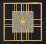
The digital transmission line requirements of the package are driven by the chip design and performance requirements. The clock circuits are typically single-ended and use a microstrip with a 50  impedance. Differential pairs that carry high speed signals are microstrips with backside ground only or coplanar waveguides (CPW) with both top surface and backside grounds. Figure 1 shows the StratEdge SE50 package that is capable of supporting very high speed data rates and Figure 2 shows the performance of one of the single microstrip transitions, with one ribbon bond and a 0.190" 50
  line.
line.
Mechanical Requirements
The packaging challenges come in the ability to achieve the physical requirements. The die differential pair may be ground-signal-signal-ground or ground-signal-ground-signal-ground. Typically, this is on a 6 mil pitch made up of 4 mil pads and 2 mil spacing. The package substrate pitch is driven by the metallization used. If a refractory metal is used (such as tungsten) 5 mil lines and 5 mil spacing can be realized. With gold fine line technology, 2 mil lines and 2 mil spacing is achievable.
To minimize ground bounce, noise and impedance mismatches for high speed devices, the signal grounding must be as well defined as the signal traces. The issue is how the die's ground is connected to the package ground. The ground traces are on the top of the die but most high speed devices do not provide a backside ground. Having the grounds on the top of the die allows for wafer probing but they must still be connected to the ground of the package. The package must then have ground pads on the substrate top and still be connected to the base. This connection is realized with vias, castellations, traces or down bonds. The package manufacturer's processes drive the choices available.

Next, the package is connected to the board ground. A cutout in the board can be used to mount the package to the board metal. Figure 3 shows a design for a device-to-package transition. The package substrate has microstrip differential pair transmission lines. There are ground pads on the substrate that are connected to the package ground using castellations. Figure 4 is an Ansoft HFSS model of the structure. The model was simulated up to 100 GHz and then converted to a SPICE model using Ansoft Full Wave Spice. In SPICE, the structure was simulated with a typical 40 Gbps pulse. The substrate was modeled and found to be a low loss, well-matched structure.
Another major concern is how to connect the die pads to the package traces. The choice is driven by the bonding equipment available. Both wire or ribbon bonds can be used. To minimize the inductance, the loop height must be kept as low as possible. The more the wire looks like a continuation of the microstrip transmission line, the better. With ball bonding, the bond from the ball must first go up and thus creates too high a loop height. Wedge-to-wedge bonding is preferred because the wire can be kept very flat and parallel to the substrate. First, single wire bonds from the die pads to the traces were tried. The output pulse displayed ringing and did not achieve the 10 and 90 percent voltage requirements of a logical 1 and 0 for a 40 Gbps signal. Next, a 3 mil wide by 0.5 mil thick ribbon was tried. The ribbon is known to provide better performance because it allows the bond to look like a continuation of the microstrip transmission line. Figure 5 shows that the input and output waveforms are virtually the same. The only problem is that most companies do not have fully automatic ribbon bonders but do have fully automatic wire bonders. Therefore, to utilize wire bonders and achieve the required performance, two parallel wires can be bonded at each interconnect and thus reduce the total inductance. Figure 6 shows the response for this configuration. The output signals are detectable and this configuration will work for OC-768 data. The analysis reveals that the largest mismatches occur at the mechanical interconnects; therefore, repeatable chip placement and wire bonding are an absolute must to guarantee repeatable performance.

The package and die assembly issues are next to be resolved. The die must be positioned in the package cavity logically to address the location of the high speed pairs. With the use of as-fired ceramics in StratEdge packages, a 1.5 mil gap is typically the maximum distance between the device edge and the package cavity edge. But it is difficult to achieve a 1.5 mil gap on all four sides of the die. There needs to be room for assembly tools such as a collet or tweezers when mounting the die into the package. It is recommended that the die have no more than two sides with microwave or high speed digital lines to maintain minimum gaps. Figure 7 shows a leaded high speed digital package with two sets of differential pairs on each side. The top and bottom traces are for biasing and have a much larger gap between the die and the substrate to aid in handling during assembly. Another issue is the height of the device and thickness of the package substrate. The die thickness varies from 2 to 25 mils depending on the material used, while package substrates are typically from 10 to 15 mils thick. The final issue is the method of wire bonding. As discussed earlier, wedge-to-wedge bonding is preferred with two 1 mil wires or ribbon for the high speed and microwave connections.

Integration
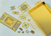
In optoelectronics modules, most of the electrical functions are in separate housings (the laser in one housing with the detector circuitry in another, for example). Future integration will require more functions to be combined, and optics and electronics will begin to share packaging. The electrical interconnects can be made in a number of ways, including feed through in a metal box, leads through a glass sidewall, a ceramic package with metallized traces and a connector in a metal or glass wall box. The optical fibers can be brought in with a metal pipe or be brazed or glassed into the package. A number of high speed digital package solutions are illustrated in Figure 8 , including leaded, leadless, surface-mount and fiber optic tube.

Conclusion
Electronic packaging possesses numerous technical challenges that have plagued design and process engineers. For high speed digital packaging, the transmission lines have microwave requirements and the interconnects must be well maintained to guarantee electrical performance. The assembly methods must be understood and controlled to aid in the proper layout of the circuit. Fortunately, there are technology solutions available today to package both electrical and optical high speed components for volume production.
References

1. J. Carter and A. Lindner, "Microwave Circuits Require Special Packages," Electronic Packaging & Production , November 1996, pp. 43-48.
2. J. Carter and A. Lindner, "Packaging Requirements for GaAs MMICs," Compound Semiconductor , Vol. 6, No. 9, December 2000/January 2001, pp. 66-69.
3. L. Levine, "Wire Bonding Optoelectronics Packages," Chip Scale Review , Vol. 5, No. 8, November/December 2001, pp. 49-53.
4. A. Lindner, "Specialized Packaging Demands for Microwave, Millimeter-wave and High Speed Digital Circuits," Future Fabrication , Vol. 1, No. 2, 1997, pp. 369-371.
5. W. Oldfield, "Connector and Termination Construction Above 50 GHz," Applied Microwave & Wireless , Vol. 13, No. 4, April 2001, pp. 56-66.
Alan Lindner received his BSEE degree from Arizona State University and his MSEE degree from San Diego State University. He is a senior member of the IEEE Microwave Theory and Techniques Society and holds five patents in packaging. He is currently employed at StratEdge Corp. as the head of the design and test department developing microwave, millimeter-wave and high speed digital packaging. Previously, he worked at Teledyne Ryan Electronics as a design engineer and a manufacturing program manager of radar navigation systems.
