
The march of technological progress continues as traditionally bulky and discrete microwave devices become integrated in increasingly smaller microelectronic modules and packages. New high performance GaN, GaAs, InP and other Class III-V and silicon semiconductor devices, along with high performance silicon variations such as SiC, are designed to push performance and enable new communications and sensing applications. As examples, active electronically scanned array radar and long-range, high throughput unmanned aerial vehicle telemetry are possible due to advances in RFICs and MMICs.
As with most advancements in technology, the steps forward come with design challenges. These challenges may be unknown and impossible to predict until the devices are shipped and integrated in new assemblies and systems. Often, enhanced features, integrated capabilities and heightened performance make the semiconductor die more expensive, and the loss of any die becomes a significant issue. This has been the case for a new generation of thin compound semiconductor die. BAE Systems, a global aerospace and defense technology company, and Gel-Pak, a division of Delphon, have investigated the loss of millions of dollars from “cost of poor quality incidents” caused by die migration in waffle pack trays, known as component out of pocket (COOP) defects. Their study revealed that while die migration occurred during customer handling of the waffle packs and chip trays, a significant amount occurred during the packaging by the supplier and subsequent transit to the customer. The wide flatness tolerances between the tray and the lid of traditional waffle packs, which far exceed the thickness of the thin semiconductor die, was the principal culprit.
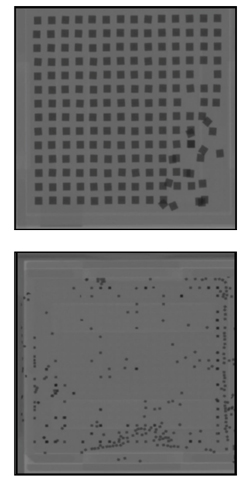
Figure 1 X-ray images of COOP with a traditional waffle pack.
This article discusses the joint study between Gel-Pak and BAE Systems and the development of a Lid-Clip Super System (LCS2™) to reduce die migration. The LCS2 protects extremely thin die, down to 2 mils (50 μm), during the jostling which occurs during handling and transport by semiconductor manufacturers, their distributors and customers around the world.
REDUCING DIE THICKNESS
Organizations from DARPA to cellular operators have invested in advanced semiconductor processes to enhance the performance of RFICs and MMICs, performance advantages such as higher power density, higher frequency coverage with wider bandwidth, improved linearity, lower noise and more integration. These developments have led to more compact ICs while integrating more signal chain components and features on the same chip, created a system-on-chip. These new processes operate through the microwave frequencies and into the mmWave spectrum, enabling new systems for communications, automotive, satellite and defense.
Lowering the cost, weight and size of the semiconductor devices helps to enable new systems. One aspect is reducing die thickness, which reduces the thermal resistance between the device junction and the conductive path that removes the heat. The RF performance may also benefit from thinner die, with lower parasitics that extend the upper frequency range. Thinning techniques have been developed for compound semiconductor and silicon on insulator wafers to reduce die thicknesses for RF, microwave and mmWave applications.1–3
DIE MIGRATION
Despite the performance and integration benefits, reducing die size causes handling and transportation challenges. COOP refers to a die in a waffle pack escaping its pocket, possibly moving to the pocket of another die (see Figure 1). This migration is inconvenient and costly. Die in the same pocket may become damaged as they bounce and grind against each other. A die may flip, changing its orientation and causing placement errors with automated handling equipment. Die may become lodged between pockets, damaged by the waffle pack or migrate to another pocket when the waffle pack is opened. COOP degrades the quality of the manufacturing process, causing
- Component damage and scrap
- Additional labor to inspect and reorder components
- Manufacturing delays from yield loss and interrupted production
- Reduced pick-and-place machine utilization
- Additional quality management administration
- Over-engineering the automated assembly process.
Die migration will increase manufacturing cost. Since the cost of MMICs and RFICs is substantial, losing even a few from COOP can add thousands of dollars from damage, scrap and non-value-added labor. The worst-case scenario occurs when a defect from migrated die is not caught until after die placement in the next higher assembly, adding the cost and delay for troubleshooting and rework.
ROOT CAUSE
Historically, the cause of die migration has been attributed to handling when opening the waffle pack, although there was little investigation of the end-to-end process of handling, packaging, storing and transporting semiconductor die. When traditional waffle pack chip trays were designed, die were thicker, i.e., hundreds of micrometers. In the late 2000s, die thickness began to shrink below 250 μm and is now in the tens of micrometers. Yet the industry made little change to die packaging practices for waffle packs, which increased COOP losses. Not surprisingly, device suppliers and their customers saw each other as the cause of the increasing problem. Use of X-ray and 3D measurement systems have led to more accurate identification of root causes, and there are many:
- Lack of awareness of Entegris’ literature describing warpage and the potential for migration
- Carbon loaded polypropylene lids and trays with a 0.012 in. warpage specification
- ABS and carbon loaded polycarbonate lids and trays with a 0.004 in. warpage specification
- Irregular deformation of lids and trays caused by the standard one-piece clip
- Non-woven polyethylene inserts misaligned and pinched during assembly, creating escape paths
- Components not flat in the chip tray before lidding
- Stacked components, i.e., two or more components in a single pocket due to operator error or warped lids
- Operator-dependent assembly process
- Application of label to bottom side of waffle tray by customers requires removal of the clip
- Worn or broken one-piece clip
- Bump lid failure from improper use and warpage.
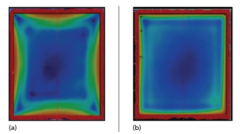
Figure 2 Measured internal surface flatness of carbon loaded polypropylene (a) and carbon loaded polycarbonate (b) lids.
To improve the knowledge of COOP with the goal of reducing it, VJ Electronix developed an X-ray counter system (XQuik II) for BAE Systems in 2017. The XQuik II can view and count the components within a sealed waffle pack during receiving inspection and identify COOP before the waffle pack is opened. Data from the XQuik II system showed substantial levels of COOP when waffle packs were received by BAE Systems, prior to opening the waffle packs. This showed that COOP occurs at the supplier and during transit, not only during customer processing. COOP was found with 23 different suppliers, leading to the conclusion that semiconductor suppliers are unaware they are shipping waffle packs with COOP, as few suppliers use X-ray systems to inspect outgoing waffle packs.