
In the past few decades, the wireless industry has been driven by constant innovations and transformations due to introduction of wireless communication standards such as 4G LTE, 5G, Bluetooth, Wi-Fi and many more.1 These advancements in the wireless industry coupled with rapid manufacturing techniques requires advanced product design that involves complex multi-physics considerations. Competition in consumer electronics market calls for measures to improve product performance with lowering the development cost and at the same time significantly reducing the time-to-market. All these challenges can be addressed by simulation-driven virtual prototyping to reduce the physical testing.2-4 Moreover, the simulation-driven virtual prototyping can be employed for designing modern smart products in order to accelerate product development speed, ensure intrinsic product qualities and improve decision-making process during the development cycle. Therefore, the simulation-driven design can be one of the important factors contributing to product completeness and timely market launching of smart products.
I. Introduction
Figure 1 shows a product development process for a smart speaker which consists of a speaker component, Printed Circuit Board (PCB), assembled electric components, and the final product with a speaker cabinet. For the smart speaker’s development, a three step simulation-driven virtual prototyping methodology is applied in this article. The first step is to design, verify and analyze the PCB layout design, the second step is design and integration for the Bluetooth antenna embedded on the PCB and positioned inside the speaker cabinet, and the third step is the smart speaker’s wireless communication performance evaluation by considering neighboring wireless products.
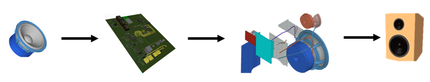
Speaker PCB Assembled electronics Final product
Figure 1. Product development process for a smart speaker.
This article is organized as follows. In section II, PCB design concept and main functions for a smart speaker are introduced and explained. Subsequently, rule-based verification and signal integrity (SI)/thermal analysis methods are applied to upgrade the product’s electric performances such as noise-free audio qualities and high-speed data exchange. In section III, miniature techniques are utilized to design for a Bluetooth antenna on the PCB. Besides, the designed antenna is tuned for the integration on the PCB and then the position of the PCB inside a speaker cabinet is studied for optimal performances. In section IV, the smart speaker’s wireless communication performances are simulated to evaluate the quality of the product in realistic operating environment. Particularly, the Bluetooth’s coverage of the smart speaker is estimated by calculating network parameters (data rate and throughput) as well as interference effects due to the smart speaker with other wireless devices inside home environment. Section V summarizes with conclusions.
II. PCB Design, Verification and Analysis
PCB design for smart speaker
The current generation of smart speakers receives audio signals wirelessly using radio frequency waves. One of the most popular radio frequency standards that supports audio transmission to speakers is – Bluetooth (BT).5 The basic building blocks of a smart speaker include the wireless section (mostly Bluetooth), the charging circuitry, audio amplifier for quality audio output, a user informative output (e.g. Liquid Crystal Display, LCD) and the main controller with the memory, providing a reliable connection between these blocks. Further additions are made to enhance the feature list. A block diagram representation of a basic smart speaker is shown in Figure 2. To understand the electrical operations of the smart speaker, power supply flow is drawn in red from the USB connector toward the other functional blocks. Similarly, the blue line and green line indicate the digital signal and audio signal exchange among the blocks, respectively.
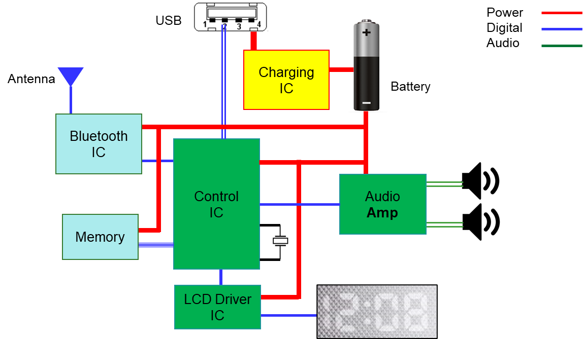
Figure 2. Block diagram of a basic smart speaker.
When designing a high-quality smart speaker, aspects such as the quality of audio signal, Bluetooth antenna performance parameters and interference with other wireless signals must be taken into consideration. The PCB with the electronic circuitry including Bluetooth IC and the antenna is shown in Figure 3. This is a 6-layer PCB with dimensions 106 x 137 mm and a total thickness of 0.7 mm. Main functionalities of PCB are audio amplifiers for high quality audio output, memory IC for storing wireless information such as pairing details and battery status, and for smart applications, USB connectivity for charging or diagnosing, charging and power supply circuitry, Bluetooth for wireless connectivity, LCD driver and display module to provide more information to the users. Lastly, the microcontroller administers the synchronous functionality of all different parts of the PCB.

Although there are specific ICs which make sure each of the functionalities are operational, there are certain other parts on the PCB which are equally important and decide the reliability of the system. Some of them, viz., the differential nets in audio lines, the connectivity between the controller and the memory IC namely, clock, address, command and data lines, the differential data lines from USB to the controller and the custom antenna for the Bluetooth module, are crucial in determining the quality and efficiency of the smart speaker. A 3-D view of the board is shown in Figure 4, highlighting some of the essential nets such as audio lines, USB lines, and memory lines.

Figure 4. 3-D view of the PCB.
The nets marked with ‘audio lines’ are a differential pair. To ensure superior audio output, the differential lines have to match a certain specification of differential pairing. Also, the lines must be shielded with electrical ground to avoid noise seeping into them from other sources. The ‘memory lines’ and ‘USB lines’ must follow their individual high-speed protocol for a seamless experience. Specifically, the high-speed lines should satisfy their required impedances based on their speed and frequency of operation. Moreover, the memory lines must follow their DDR (Double Data Rate) specification to avoid discrepancies in data transfer to and from the memory IC. Lastly, to avoid costly design iterations and over-design, and for the general safety of the device and the user, the PCB must be checked for its thermal behavior and correct thermal anomalies, prior to manufacturing.
PCB design verification and analysis
As discussed earlier, the layouts of the audio line, USB line, and memory lines need to be carefully designed for the smart speaker’s reliable operations. Therefore, to ensure the electric qualities related to the PCB layouts, PCB verification and analysis methods are applied. The target PCB layouts for the verification and analysis are the differential audio lines and the high-speed lines (USB interface and memory bus lines) exclusively shown in Figure 5. To verify the differential audio line’s layout, rule-based electric checker, design for electric (DFE) supported in Altair PollEx,6 is utilized. Signal integrity (SI) analysis is conducted to evaluate the PCB layout for the high-speed lines with respect to transmitting and receiving digital signals’ waveforms and voltage/time margins. In addition to SI analysis, thermal characteristics of the PCB board are analyzed. The thermal analysis checks for excessive component temperature and uneven board temperature at an early design stage.
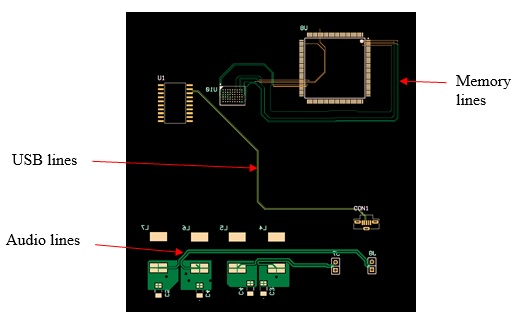
Figure 5. Exclusive view for PCB layouts to be verified and analyzed.
The differential audio lines whose width is 0.5 mm are evaluated with respect to the paired lines’ separation and coupling rate because two positive and negative lines should be tightly coupled within a specific distance. In Table 1, the separation criterion (center-to-center distance, 0.75 mm) is determined by adding the line width (0.5 mm) and the addition space (0.25 mm) and the coupling rate criterion (better than 80 percent) is determined by considering the structures of the USB IC and connector. From the verification solver, it is obtained that the maxim separation (0.893 mm) between the two lines and the coupling rate (76.6 %) does not satisfy the criteria. Additionally, the ground shield ratio showing how much the audio lines are shielded by a ground plane meets the criterion (over 80 percent). These results can be useful for a PCB designer to decide whether modification of the layout for the audio lines should be made or not.
Table 1. DFE results for the differential audio line.
|
|
Separation (mm) |
Coupling rate (%) |
Ground shield ratio (%) |
|
Criterion |
= 0.75 |
> 80 |
> 80 |
|
Verified |
0.893 |
76.6 |
Pass |
In Figure 6, the characteristics of the USB data lines (D+/D-) are studied by the waveforms at the transmitting and receiving ports. The ideal digital signal whose pulse width is 2.08 ns (Data rate: 480 Mbps) and whose peak voltage is 0.4 V is transmitted from the USB IC and received at the USB connector. By comparison of two signals, it is observed that the received signal has a time delay which accounts for the USB lines’ length. Furthermore, the receiving signal has enough voltage margins for the USB normal operation because the high threshold (0.3 V) and low threshold (0.1 V) of the USB 2.0 specification are satisfied. For more exact compliance test, eye diagram of the received signal should be drawn and estimated with the eye mask defined by the USB 2.0 specification.7
 Figure 6. Signal waveforms for the USB data line: (a) Transmitted signals at USB IC, (b) Received signals at USB connector.
Similar to the previous USB data line analysis, the memory interface lines between the controller and the memory (Pseudo SRAM: Static Random Access Memory) are analyzed using the SI solver in PollEx and shown in Figure 7. For this analysis, one differential clock line and a group of address lines are selected from the PCB design. The controller is assumed to send the clock signal whose frequency is 133 MHz and the address signals whose data rate is 256 Mbps. The eye diagram is obtained at the memory ports. The clock signal is used as a criterion to estimate the interface with the eye mask whose high and low thresholds are 1.3 and 0.4 V, respectively. Additionally, it is assumed that the required setup time and hold time for the interface are 2 and 1.5 ns. From the eye diagram showing enough voltage margin, it can be concluded that the interface lines are well routed for the safe 256 Mbps data exchange between the controller and the memory.
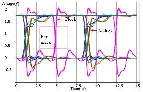 Figure 7. Eye diagram for the clock and address lines of the memory bus
Board-level thermal analysis is performed to check the main audio amplifier’s temperatures in operation by using the data sheet’s specification about the audio amp’s power rating at room temperature, 5 W and its package type, QFP (Quad Flat Package). Figure 8 shows the temperature contours in two convection conditions: one is natural convection, and the other is forced air convection whose air flow’s velocity is 5 m/s. In the condition of the natural convection, the highest temperature, 850 Celsius which is recorded below the amplifier is the maximum allowable value for the amplifier’s normal operation. As a remedy for the high temperature, the forced convection is proposed to decrease the temperature from 850 to 590 Celsius to ensure a reliable operation condition for the audio amplifier.
 Figure 8. Thermal contour plots on the surface of PCB: (a) Natural convection, (b) Forced air convection (5 m/s).
III. Antenna Design and Integration
In this section, concept, design and placement of the Bluetooth antenna for the smart speaker is discussed. Bluetooth operates at frequencies between 2.402 and 2.480 GHz. The antenna used should have reflection coefficient of at least -10 dB in this frequency band. These parameters are crucial to validate the performance of antenna. A meander line antenna (MLA) proposed by Rashed and Tai8 to reduce the resonant length of the antenna is applied. Subsequently, the designed antenna was integrated on the PCB. The PCB is placed in its real working environment in the speaker assembly to identify the optimal location. This section demonstrates the electromagnetic characteristics of the antennas in different configurations given by changing the location and orientation of the PCB inside a speaker cabinet using commercially available electromagnetic simulation tool, Altair Feko.9
Antenna design and integration on PCB
Meandering the antenna increases the path over which the surface current flows and that results in reducing the size of the antenna. The resonant frequency of a meander line antenna is a function of meander separation and meander spacing. If meander spacing is increased, the resonant frequency decreases. On the other hand, if the meander separation is increased, resonant frequency decreases.10 To validate the concept, we simulated a meander line antenna on a bare PCB as shown in Figure 9.

(a)
 (b)
(b)
Figure 9. Designed BT antenna in free space: (a) Meander line antenna’s shape, (b) Reflection coefficient.