
ALLEGRO & AWR WORKFLOW
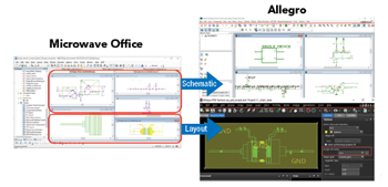
Figure 4 Allegro RF to PCB workflow using the V16 import wizard.
Moving from the IC to the board, an RF to PCB workflow starts with the creation of unified libraries and technical files from Allegro parts and board definitions. The new unified library import wizard in V16 software reads the Allegro symbols and footprints in the universal library and technology file and converts this data into an AWR PDK that can be used to create an RF design using standard design entry and simulation methods. After completing the design, the RF engineer exports the schematic and layout of the subcircuit with all the underlying hierarchy into a unified library design using a new utility in AWR V16 software (see Figure 4).
On the back end, the layout engineer needs access to the uncompromised data designed to the company approved bill of materials (BOM) and target manufacturing process. Starting with Allegro-sourced component parts from an organization’s approved BOM and process technologies, the RF engineering and layout teams can then improve design hand-off efficiency and reliability while reducing the back and forth to reconcile differences between RF design and manufacturing requirements.
MULTIPHYSICS

Figure 5 Microwave Office V16 provides large scale EM analysis using Clarity.
Historically, large RF structures, such as phased-array feed networks, have been manually sectioned into smaller structures for analysis using the largest and most powerful computing resources. The Clarity 3D Solver 3D EM simulator, used for designing critical interconnect, RFIC, MMIC, module, PCB and SoC designs, overcomes the limitations of legacy EM analysis software by leveraging Cadence’s distributed multiprocessing technology, which delivers virtually unlimited capacity at 10x the speed. Now integrated within AWR software, the Clarity 3D Solver provides RF designers with ready access to high capacity EM analysis for design verification and signoff of large, complex RF/mixed-signal systems, with capabilities beyond those offered by the AWR AXIEM 3D planar and AWR Analyst 3D finite element method (FEM) solvers.
Clarity integration with the Microwave Office platform is an automated process where the entire analysis is fully within the AWR environment. Once simulation is complete, a dataset with input geometry, simulation setup and S-parameter results is automatically assembled and associated with the given EM document for plot, measurement and subsequent extraction, circuit simulation, tuning and optimization. The link supports mesh, current and field visualization data in addition to S-parameters, enabling designers to use the rich set of EM 3D annotations already in the AWR Design Environment platform (see Figure 5).
THERMAL ANALYSIS

Figure 6 Coupled electrothermal analysis with Celsius Thermal Solver.
IC and electronic system companies, particularly those using IC packaging and/or multi-technology modules, face thermal challenges that can derail project schedules. The Cadence Celsius Thermal Solver within AWR software offers a solution for RF device, PCB and module designs supporting electrothermal analysis using model information sourced from AWR Microwave Office software, using existing MMIC design data and geometries such as layout, material properties and power source values from the RF simulation. The solver provides a full IC temperature profile at the relevant resolution of the IC layout, available as a graphically viewable 3D temperature overlay, as well as a temperature-annotated netlist for circuit simulation, as shown in Figure 6.
Thermal analysis provides insight regarding the operating temperatures that can degrade RF performance and threaten device reliability. By using model and power dissipation information obtained from Microwave Office software directly in Celsius Thermal Solver, designers can achieve better accuracy. Additional objects such as a heat sink can be added to the die and exported as a new structure for thermal analysis, which enables designers to investigate heat sinking strategies to best manage heat.
SUMMARY
As RF-enabled systems proliferate and adopt heterogeneous technology integration for greater functionality in smaller footprints, design platforms and multi-technology workflows must be interoperable. The AWR Design Environment V16 platform encompasses innovative functionality increasing engineering productivity through seamless cross-platform and multiphysics integration of the AWR platform RF/microwave design IP within the Virtuoso and Allegro design platforms, as well as EM and thermal analysis of complete large-scale designs through Clarity and Celsius solvers.
Engineers working from the IC through the system can better address cross-fabric, multi-technology product development challenges within the comprehensive front-to-back RF workflows offered by Cadence. AWR V16 is further streamlining product development and user productivity, eliminating inefficiency and lost insight when designers spend unproductive time and cycles switching among siloed tools.
Cadence Design Systems, Inc.
San Jose, Calif.
www.cadence.com