Figure 4 ADS Modelithics PMA-5451+ model using 20 mil RO4350B substrate.
Modelithics provides models for many Mini-Circuits components, including the PMA-5451+ LNA. The model is a data-based behavioral model developed from broadband S-parameters and noise parameters measured using a Keysight PNA-X vector network analyzer equipped with the ultra-fast noise option. The Modelithics model for the PMA-5451+ is validated for S-parameters and noise parameters at +25°C and biased at +3 V and 30 mA, predicting the S-parameters from 45 MHz to 20 GHz and noise parameters from 500 MHz to 8 GHz—beyond the operating frequency range specified by Mini-Circuits. The model includes three substrate options, since it was extracted from measurements performed using 6.6, 10 and 20 mil thick Rogers RO4350B substrates. Designers can select one of these substrates using the “Substrate” parameter. For this design, the 20 mil thick RO4350B was used. Modelithics provides a datasheet for the PMA-5451+ showing the application schematic used for model extraction. Also included are the model’s S-parameters and noise parameters. The plots from the model datasheet can be replicated by simulating a schematic in ADS containing the PMA-5451+ model with 50 Ω port terminations at the input and output (see Figure 4).
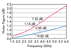
Simulating the schematic of Figure 4, the actual noise figure (NF50 in the model datasheet) and minimum possible noise figure (NFMin in the model datasheet) are plotted in Figure 5, and Figure 6 compares the simulated 50 Ω noise figure with the three substrate thicknesses available in the model. Figure 5 shows the noise figure is 1.14 dB at 3.3 GHz, rising slightly to 1.32 dB at 3.8 GHz. At these same frequencies, the minimum noise figure is 0.82 dB and 0.89 dB, respectively. At 3.3 GHz, the noise figure is 0.32 dB higher than the minimum, with a greater difference of 0.43 dB at 3.8 GHz. By designing a proper matching network, the LNA can be optimized so the noise figure is closer to the minimum values; a realistic goal is a noise figure ≤ 1.0 dB from 3.3 to 3.8 GHz.

Figure 5 Simulated 50 Ω noise figure (red) and minimum noise figure (blue).

Figure 6 Simulated 50 Ω noise figure using 6.6 mil (red), 10 mil (blue) and 20 mil (green) RO4350B substrates.
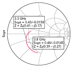
The optimum source reflection coefficient for the minimum noise figure, known as Sopt in ADS, can also be determined (see Figure 7) and seen in the Modelithics model. To achieve the lowest noise figure, the matching network placed at the input of the PMA-5451+ must produce a source reflection coefficient, ΓS, closely matching Sopt over the frequency range of 3.3 to 3.8 GHz. Figure 8 plots the |S21|, |S11| and |S22| from the same simulation, showing the gain varies between 8.70 and 9.82 dB over the n78 band.

Figure 7 Optimum source reflection coefficient for minimum noise figure, 1.5 to 6 GHz.

Figure 8 Simulated |S21| (a), |S11| and |S22| (b).
MMIC LNA DESIGN
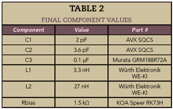
The ADS schematic for the MMIC LNA design, shown in Figure 9, essentially mirrors Mini-Circuits’ recommended application circuit. The design includes the PMA-5451+, capacitor C1 and inductor L2 located at the input of the MMIC. These two components combined with the microstrip interconnects connecting them to the PMA-5451+ are the input matching network. The capacitor C2 and inductor L1 at the output of the MMIC are selected to achieve acceptable output return loss. The circuit also includes a 1.5 kΩ bias resistor, Rbias, setting the 30 mA bias current, and a bypass capacitor, C3.

Figure 9 ADS model of the complete LNA design.

Figure 10 Simulated gain (red) and noise figure (blue) of the unoptimized LNA design.
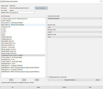
Modelithics Microwave Global Models™ are used for the capacitors, inductors and resistor, which are all 0603 sized parts. AVX SQCS capacitors are used for C1 and C2, Würth Elektronik WE-KI inductors are used for L1 and L2, a KOA Speer RK73H 1.5 kΩ resistor is used for Rbias and a Murata GRM188R72A 0.1 µF capacitor is used for C3. A single Microwave Global Model covers the full range of values for a vendor’s component, and since the values in these models are scalable, the models are useful for tuning or optimizing a design.
To optimize the noise figure from 3.3 to 3.8 GHz, the values of C1 and L2 must be suitably adjusted. As the lengths of the microstrip interconnects connecting C1 and L2 to the PMA-5451+ play a role in achieving the best performance, the optimization process includes tuning the lengths of the microstrip interconnects, as well as adjusting the component values. To establish a starting point for the design, the gain and noise figure of the LNA were simulated before optimizing the component values and interconnect dimensions, by setting C1 and L2 to the initial values of 100 pF and 390 nH, respectively, and the microstrip interconnect lengths to arbitrary values. At 3.8 GHz, the starting gain was just under 8 dB and the noise figure slightly greater than 1.6 dB (see Figure 10).

Figure 11 Discrete elements optimized with the Modelithics passive component model parameters

