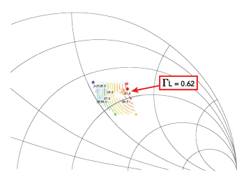
Figure 3 Device drain efficiency measured using a traditional load-pull setup, showing a maximum drain efficiency of 31.5 percent at 75 GHz. The traditional setup can’t obtain closed contours

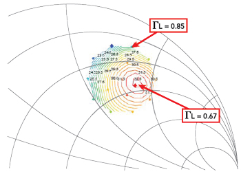
Figure 4 Device drain efficiency measured using a hybrid-active load-pull setup, which provides closed contours. At 2 dB compression, the maximum drain efficiency is 32.5 percent at 75 GHz.

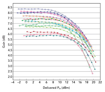
Figure 5 GaN HEMT power gain vs. load impedance measured with the hybrid-active vector-receiver load-pull system.
To date, active and hybrid-active load-pull have been limited to coaxial measurements in commercially available systems because of the impracticality of measuring and controlling the magnitudes and phases of the a and b waves using waveguide frequency extenders. To overcome this limitation, Maury Microwave has introduced custom low-loss couplers with integrated down-conversion (see block A in Figure 2), which extend VNA-based load-pull measurements to 110 GHz, and a source control unit (see block B in Figure 2) enables accurate amplitude and phase control to 110 GHz. The custom couplers enable direct a and b wave measurements at the vector calibrated DUT reference plane, increasing system measurement accuracy and providing critical device performance - output power, power gain, input Γ and power-added efficiency (PAE) - for each input power level and load impedance state. The amplitude and phase controller with the frequency multiplier and step attenuator on the load loop (see block C in Figure 2) enable 0.01 dB magnitude and 0.1 degree phase control of the a2 wave.
This hybrid-active load-pull solution enables W-Band VNA-based load-pull measurements, reaching |ΓL| = 1 at the probe tip reference plane for DUTs with output power on the order of 1 to 2 W. These capabilities enable measurements of highly mismatched devices previously impossible to characterize due to system limitations. The implementation of active load-pull using waveguide frequency extenders is possible up to 1.1 THz, frequencies where commercial automated impedance tuners are unavailable or impractical.11
DEVICE MEASUREMENTS
To demonstrate this solution, a small periphery, two finger, GaN HEMT was characterized at 75 GHz using passive and hybrid-active load-pull systems. A traditional waveguide passive load-pull system could only achieve a maximum |ΓL|< 0.62. Without closed contours (see Figure 3), the best device performance may be missed, leading to incorrect conclusions about the optimum DUT impedances. As noted, this is problematic when characterizing small periphery active devices, where the output impedance is typically close to the edge of the Smith chart. The same device PAE characterization using a hybrid-active load-pull system is shown in Figure 4. Much higher magnitude ΓL is achieved at the DUT reference plane, enabling closed contours and providing confidence the correct load impedances are identified to maximize DUT performance.
Other benefits of hybrid-active vector receiver load-pull include real-time measurements of the a and b waves at the input and output of the DUT, which enable characterizing power gain variation and input reflection coefficient versus available input power and load impedance. Figure 5 shows the measured gain variation with load impedance of the GaN HEMT. The characterization of input impedance variation is important when optimizing the power gain at a particular DUT input power level, to optimize the design of the input and output matching networks. Due to the low device gain at these frequencies, designers must consider the tradeoffs among power gain, drain efficiency, PAE and output power.
CONCLUSION
During the initial stages of device technology development, timely feedback to device development engineers is important to accelerate the development process. Quickly and accurately benchmarking the performance of various semiconductor technologies using small periphery devices contributes to reducing development costs and expediting time to market. This can be achieved using hybrid-active vector receiver load-pull systems providing |ΓL| = 1 at the DUT reference plane at E- and W-Band frequencies. The measured vector a and b waves enable the characterization of various DUT parameters, such as delivered input power, output power, power gain and PAE that are not normally available from scalar measurements. This enables higher device characterization accuracy, facilitating more accurate device parameter extraction for better model fidelity.
References
- Z. Griffith, M. Urteaga, P. Rowell and R. Pierson, “340-440 mW Broadband, High-Efficiency E-Band PA’s in InP HBT,” IEEE Compound Semiconductor Integrated Circuit Symposium, October 2015.
- H. Lin and G. M. Rebeiz, “A 70–80-GHz SiGe Amplifier with Peak Output Power of 27.3 dBm,” IEEE Transactions on Microwave Theory and Techniques, Vol. 64, No. 7, July 2016, pp. 2039–2049.
- J. A. Jayamon, J. F. Buckwalter and P. M. Asbeck, “A PMOS mm-Wave Power Amplifier at 77 GHz with 90 mW Output Power and 24% Efficiency,” IEEE Radio Frequency Integrated Circuits Symposium, May 2016.
- D. xu, K. Chu, J. A. Diaz, M. D. Ashman, J. J. Komiak, L. M. Mt. Pleasant, A. Vera, P. Sekell, x. Yang, C. Creamer, K. B. Nichols, K. H. G. Duh, P. M. Smith, P. C. Chao, L. Dong and P. D. Ye, “0.1-µm InAlN/GaN High Electron-Mobility Transistors for Power Amplifiers Operating at 71–76 and 81–86 GHz: Impact of Passivation and Gate Recess,” IEEE Transactions on Electron Devices, Vol. 63, No. 8, August 2016, pp. 3076–3083.
- D. Lammers, “RF SOI Shines for 5G Power Amps,” Global Foundries, February 2019, www.globalfoundries.com/news-events/press-releases/rf-soi-shines-5g-power-amps.
- D. M. M. -P. Schreurs, J. Verspecht, S. Vandenberghe and E. Vandamme, “Straightforward and Accurate Nonlinear Device Model Parameter-Estimation Method Based on Vectorial Large-Signal Measurements,” IEEE Transactions on Microwave Theory and Techniques, Vol. 50, No. 10, October 2002, pp. 2315–2319.
- K. Makiyama, Y. Niida, S. Ozaki, T. Ohki, N. Okamoto, Y. Minoura, M. Sato, Y. Kamada, K. Joshin, K. Watanabe and Y. Miyamoto, “High-Power-Density InAlGaN/GaN-HEMT Technology for W-Band Amplifier,” IEEE Compound Semiconductor Integrated Circuit Symposium, October 2016.
- S. Taking, D. MacFarlane, A. Z. Khokhar, A. M. Dabiran and E. Wasige, “DC and RF Performance of AlN/GaN MOS-HEMTs,” Proceedings of the Asia-Pacific Microwave Conference, December 2010, pp. 445–448.
- J. M. Schellenberg, “A 2-W W-Band GaN Traveling-Wave Amplifier With 25-GHz Bandwidth,” IEEE Transactions on Microwave Theory and Techniques, Vol. 63, No. 9, September 2015, pp. 2833–2840.
- S. Dudkiewicz and R. Hilton, “Overcoming the Challenges of On-Wafer Load-Pull Measurements at Millimeter-Wave Frequencies for 5G Applications,” Maury Microwave Corporation, Application Note 5A-070, July 2018, www.maurymw.com/pdf/datasheets/5A-070.pdf.
- C. De Martino, L. Galatro, R. Romano, G. Parisi and M. Spirito, “Hardware and Software Solutions for Active Frequency Scalable (sub)mm-Wave Load Pull,” IEEE Transactions on Microwave Theory and Techniques, Vol. 68, No. 9, July 2020, pp. 3769–3775.
