Tutorial
Fibercom Clock Timing - A Review of PLL Solutions
Bar-Giora Goldberg
Peregrine Semiconductor Corp.
San Diego, CA
The fiber optics telecommunications market (called here photonics) has experienced huge growth in the last few years. Being a two-level digital transmission format, the requirements for clocking, timing, retiming and sometimes scaling are demanding in performance and economics.
Every passage of an optical and then electrical signal through various mediums or processing steps requires retiming or clocking. Noise is always added, and noise causes jitter. Jitter corrupts the signal integrity and adversely affects the bit error rate (BER).
Many applications require the addition of auxiliary functions, such as forward error control, so the scaling of clocks must be performed as well. Functions like clock and data recovery (CDR) circuits, using phase-locked loop (PLL) circuits, are most common in photonics.
PLL technology is generally recognized as the optimum solution for generation, timing, retiming, CDR and scaling, providing the combination of agility, reliability, flexibility and economy in power, and cost. This article reviews some of the standards and design considerations, and specifically focuses on jitter, phase noise and PLL simulations and results interpretation.
Background
Every digitally transmitted signal must have a clock at its source and a synchronization circuit at the receiving end. Sometimes signals have to be retimed because, while being processed, noise and jitter are added.
These "timers" or clocks must have low jitter and the correct time skew to clock the data on the middle of its eye pattern.
Jitter is the short-term, instantaneous, time variation of a clock from its ideal position (zero crossing) in time. These variations have slow and fast spectral components at every frequency offset from the center. Very slow variation can usually be tracked out at the receiving end, but fast components cause time uncertainty, hence increasing the BER.
Noise is inherent in nature and since there are no deterministic signals in the real world, all signals have jitter. Jitter in non-return to zero (NRZ) signals can be caused by intersymbol interference (ISI), signal and channel speeds, dispersion and various filtering. This type of jitter is deterministic. The focus of this article is on the random jitter in clocks (not NRZ data) where deterministic factors will have only secondary effects. Here, jitter is the random component of clock timing.
While jitter is a time measurement, the representation of the signal's imperfection in the frequency domain is expressed by its phase noise profile. An ideal signal has energy only in one frequency component; real signals have energy that is distributed across the spectrum, as shown quantitatively in Figure 1 .

Fig. 1 Signal energy spectrum.
There is a direct relationship between jitter and phase noise; after all, jitter is the integrated phase noise across the frequency band of interest. In many high speed photonics products, this integration range has been chosen to be 12 kHz to 80 MHz; however, these are not exclusive parameter limits.
The evolution and maturity of the OC-12 and 48 standards' (622 and 2488 MHz) has also set the jitter specifications to be of the order of 1 to 4 ps rms. Better jitter implies better phase noise, which can be achieved via better oscillators or improved PLL chips. Most jitter is contributed from the close-in phase noise; however, photonics clocks generally require a wide loop bandwidth, so the VCO performance can be the dominant factor mainly in applications where the loop bandwidth must be narrower and extreme phase noise requirements become the critical parameter.
Remember that narrow band loops are much more susceptible to vibrations and mechanical motion, therefore many photonics clocks use PLL circuitry with a loop bandwidth in the tens of kilohertz, while CDRs use loops with a bandwidth of approximately 1 MHz.
Given a signal with  (fm) single sideband phase noise characteristics, the phase jitter (in radians) is given by

where
Fo = center frequency
 j = jitter in radians
f1 and f2 = frequency range of integration
Tj = time jitter
For example, if the phase noise of a specific clock integrates to 0.015 radian, at 622 MHz, then the corresponding jitter is given by

This method of calculation actually measures the jitter standard deviation ( ). Since the noise distribution is always assumed to be Gaussian, tables can be used to calculate the peak-to-peak noise for a given BER. Remember that jitter is extremely critical because the signal must be sampled (clocked) at a very accurate point. Otherwise, for a given signal-to-noise ratio, errors will occur. If, when generating the signal from a clean source, the clock is too jittery, it will, in a similar way, create a problem at the receiving side as the arriving data will jitter and be hard to sample correctly.
|
Table 1 | ||||||||
|
BER |
10-9 |
10-10 |
10-11 |
10-12 |
10-13 |
10-14 |
10-15 |
10-16 |
|
|
12.0 |
12.7 |
13.4 |
14.0 |
14.7 |
15.3 |
15.8 |
16.4 |
A common industrial specification is to meet a BER of 10-12 , which implies a standard requirement of 14 peak-to-peak (p-p) jitter. In the case above, this translates to ±27 ps. Note that a BER of 10-12 with a data rate of 2400 MHz implies an average of 1 error in approximately 400 seconds. If the transmission is in short packets the error per packet is almost nil. Other BER levels per p-p jitter can be read from Table 1 .
One can see that if the phase jitter is kept the same (in radians) for different frequencies, the time jitter will scale linearly proportional to approximately 1/Fo . For the example shown above the jitter calculated for 2488 MHz would yield 0.95 ps.
Also note that when adjusting from rms to p-p, the number of samples analyzed must be defined. This is somehow related to the lower end of the integration range. Once the jitter is assumed to have a Gaussian distribution, its peak can be assumed limitless. After a long enough wait, the jitter will cross any set deviation, so it will depend on how long a wait occurs (or how accurate the Gaussian assumption is).
In Table 1 the conversion of the BER to a number of  is a statistical term, and requires a specified number of samples. If the integration is made from 12 kHz, as indicated above, it is equivalent to saying that approximately 622 106 /12 103 ~ 50,000 samples are considered. Note that when a jitter measurement is made with a digital oscilloscope, the number of samples the measurement was taken over is always indicated. Intuitively, the p-p value increases with the number of measurements taken, and a quantitative plot can be expected to look approximately like the one in Figure 2 , where the p-p jitter has been normalized to an arbitrary value.

Fig. 2 Probability of error as a function of the number of samples observed.
As the number of measurements increases, the p-p value increases because eventually (observing over more and more time), if the distribution was really Gaussian, the instantaneous jitter could reach any value. This is something that can be seen on a digital storage scope daily. Although phase noise theory is somewhat beyond the scope of this article, some observations can be made. For example, the highest low frequency components are due to slow variation of the crystals as well as low frequency components (and flicker noise) of oscillators and digital circuits that form PLL chips. These components will have a long-term effect, for they can be tracked on the receiving side. Also, if the data is transmitted in packets that are much shorter, they will have a very marginal effect, hence the reasoning to integrate from 12 kHz only and sometimes from even higher frequencies (50 kHz is also a number often used).

Fig. 3 Second-order filter, causing a third-order loop.
Phase-locked Loops
Phase-locked loops are the technology of choice for generating accurate signals with low power, accuracy, flexibility and economy. PLL technology is very mature and achieves excellent performance with lower voltage and overall power.
A PLL includes five basic functions: crystal reference, VCO, phase detector, divider and loop filter. Most PLL circuits designed for photonics timing use a third-order loop design (second-order filter, see Figure 3 ), while CDRs use second-order loops. A PLL is a closed loop negative feedback mechanism used as a most efficient and economical frequency multiplier and tracking filter.

Fig. 4 PLL block diagram.
The output frequency is  o =NFr , with good control of noise profile. In the block diagram shown in Figure 4 , the VCO is modeled as an integrator Kv /s, the loop filter is F(s) and the phase detector has a constant of Kd A/radian.
For photonics applications (SONET), the crystal oscillator will usually be at 19.44 MHz (or multiples) and N a relatively low number. A typical PLL chip for photonics applications is shown in Figure 5 , where the prescaler and main counter provide the divide by N functions, the R (reference) counter does the reference divide, and the phase detector outputs control the voltage through a charge pump which drives the loop filter. The advantages of a PLL are its low power, economy and ability to multiply frequencies efficiently.

Fig. 5 Typical PLL chip diagram.
Comparison with PLL Alternatives
There are various products on the market that generate fixed clock frequencies by using fundamental crystals or crystal multipliers. Crystal oscillators are very economical up to a fundamental frequency of approximately 40 MHz. Higher frequency crystals are either more expensive or use harmonics of the fundamentals. Active multiplication of crystals (following the crystal oscillator by a multiplier) requires excellent filtering of all unwanted harmonics and raise the noise floor as active multipliers have no inherent filtering mechanism that is natural in a PLL. In addition, multipliers are larger, bulkier and consume much more power; hence, the PLL has become the de facto controlling frequency multiplying technology. The one advantage multipliers have is close-in phase noise, which is only corrupted by the multiplication ratio of the original crystal, 20logN.
PLL Noise Characteristics
A PLL has its own noise mechanisms. The majority of random noise in photonic timing devices comes from the PLL phase detector/charge pump (CP) circuits and the VCO.
The CP noise is multiplied by the PLL transfer function, which acts like a band pass filter (in baseband analysis, it looks like a low pass filter). This is the inherent multiplying and filtering effect of a PLL. The VCO noise is multiplied by the loop error transfer function, which has a "high pass" characteristic. This is one of the great features of a PLL - the VCO noise close to the carrier is heavily attenuated. Thus, the combination of "cross over" filtering CP and VCO produces a convenient spectral control and a low noise floor.

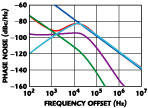
Fig. 6 Simulation of the noise properties of an OC-12 clock generator.
The plot in Figure 6 shows a simulation of an OC-12 photonics clock generator from a 19.44 MHz crystal, assuming that the VCO has a noise profile,  (fm), that is -115 dBc/Hz at an offset of 100 kHz from the carrier. This is a benign requirement for a 600 MHz VCO.
The CP noise performance is also assumed to be mediocre. The plots show the crystal noise (green), the CP noise (magenta), and the VCO noise (open loop (blue) and close loop (cyan)). The red line is the composite phase noise performance.
This design (integrated from 12 kHz to 80 MHz) yields a jitter of 0.75 ps rms. Note that for this design, with a loop bandwidth of approximately 20 kHz, the noise above 100 kHz offset is controlled by the VCO.

Fig. 7 Simulation of the noise properties of an OC-12 clock generator with improved CP noise.
Note also that the majority of the jitter energy comes from the low frequency noise components. Once the phase noise slope starts to roll off, the incremental jitter energy is low in comparison. Figure 7 shows what happens if the PLL chip is much better and has a 15 dB improved CP noise. The jitter has improved to 0.5 ps and the VCO starts to have an effect at much lower offsets.
Figure 8 shows the original design but assumes a VCO with a phase noise profile that is 15 dB worse than before. The jitter has increased to 2.5 ps and the VCO noise has become quite dominant.

Fig. 8 Simulation of the noise properties of an OC-12 clock generator with degraded VCO phase noise.
The jitter performance is thus controlled mainly by the VCO performance and the overall PLL noise. The more critical the jitter specifications become, the more improvements in VCO technology and CP noise are necessary. For ultimate performance, the VCO will have to be very good (SAW or DRO type) and the PLL loop very narrow.
An integrated (single chip), state-of-the-art clock generator, using a high Q, LC oscillator on-chip for OC-48 (2488.32 MHz) generates the phase noise profile shown in Figure 9 .
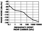
The jitter is of the order of 0.5 ps rms. This simulation assumed a super performing, extremely low CP noise, PLL chip2 . The phase noise of an actual OC-48 signal was measured on a PE3335 chip2 with a resistor at the Vdd pin 13 to drop the line voltage from 5 to 3.1V and is shown in Figure 10 . The integrated phase jitter (12 kHz to 80 MHz) is calculated to be approximately 0.13 ps rms.

Fig. 9 Simulated phase noise of a state-of-the-art OC-48 clock generator.

Fig. 10 Measured phase noise of an OC-48 signal.
Jitter vs. Phase Noise
Jitter and phase noise are a very similar representation of the same phenomenon - the imperfection of timing devices from the ideal zero crossing time location. One (jitter) measures the behavior in time and represents an integrated measurement, while the other measures the accurate noise profile in the frequency domain and allows the design, analysis and measurement of the exact noise profile.
Which one to use? It is the user's choice based on individual preference. However, the practical fact is that phase noise is much easier to measure (by almost any synthesized spectrum analyzer), while jitter measurements are more complex, require more expensive test equipment and are limited to 1 ps rms. Some exclusive instrumentation can go down to 0.25 ps but it does not come cheap.
Therefore, many engineers in the discipline prefer to use a spectrum analyzer not only for absolute measurements, but also for comparative analysis. How do you otherwise compare between competitors who demonstrate 1ps jitter?
The conversion between phase noise and jitter is quite straightforward as it includes only an integration process. Since phase noise is usually given in decade increments, some assumptions must be made for the points in between. Most CAD programs assume a linear-log approximation.
The CAD used in this article (Mathcad) actually does not need to approximate since all data points are available from the simulation

Conclusion
Jitter and phase noise are complex concepts that are interrelated when measuring and evaluating jitter requirements for timing circuits. Though most specifications for fiber-communications products are given in the time domain, measurements can be done, and in fact are easier and more economical in most applications, in the frequency domain.
Time jitter is a parameter that usually includes contribution from deterministic sources (such as channel-limited bandwidth and intersymbol interference) and, in addition, random, stochastic noise components, the focus of this article. All signals are narrow band noise. There are no deterministic signals in the real world. Jitter and phase noise determine one of the more important parameters of signals and their proximity to the ideal, one whose zero crossing timing is infinitely accurate.
Photonic timing devices, their generation and evaluation are emerging applications for signal generation with challenges in jitter performance, size, power and cost. While quite mature for OC-12 speeds, the technology is now maturing for the OC-48 speeds and starting to evolve for the 10 GHz requirements of OC-192.
Improving jitter is a lasting challenge, especially as power, voltage, size and increased rates challenge the technologies. Lower voltages forced by smaller microelectronics geometry make VCO design harder. It is believed that most of these products can and should be integrated on chip and be available as IC solutions in the near future. In parallel, better VCO technology, PLL chips and better materials will continue to advance the state-of-the-art.
References
1. T11.2 Technical Report, "National Committee for IT Standardization (NCITS)."
2. Data Sheet for PE3335, "Peregrine Semiconductor PLL Chip."
3. M. Li and J. Wiltrup, "Signal Integrity: How to Measure it Correctly?," Wavecrest Corp.
4. W.P. Robbins, Phase Noise in Signal Sources , Peter Peregrinus, London, 1982.
5. B.G. Goldberg, Digital Frequency Synthesis Demystified , LLH Publishing, 1999.
6. Peregrine Semiconductor, AN 13, "Phase Noise Demystified."

