
EXAMPLE REPULSIVE CASIMIR FORCE INSPIRED RESISTIVE CONTACT MEMS SWITCH
Figure 6 shows an example MEMS switch incorporating metamaterial cells to provide a repulsive Casimir force between contacts of the switch. This metamaterial inspired MEMS switch is formed in a coplanar waveguide (3201) having two ground planes (3202 and 3204) formed above a substrate (3205). The ground planes are separated by a channel and a signal line (3210) that is formed lengthwise in the channel. The signal line includes an input port (3212) through which a signal is received (arrow in) and an output port through which the signal is transmitted (arrow out).

Figure 6 An example MEMS switch incorporating metamaterial cells in order to provide a repulsive Casimir force between contacts of switch: (a) top-down view of the switch, (b) perspective view of the switch, (c) bisected cross-sectional perspective view of the switch and (d) side view of the switch in a closed position.

Figure 7 The split ring configuration.

Figure 8 The transmission and reflection characteristics of composite structure example #1.

Figure 9 The transmission and reflection characteristics of composite structure example #2.

Figure 10 The transmission and reflection characteristics of composite structure example #3.

Figure 11 Shows plots of reflection characteristics for a metamaterial cell with varying parameters G, S and W, given in Figure 7.
This MEMS switch includes a cantilevered beam that moves in and out of the plane of the coplanar waveguide in order to move in and out of contact with the signal line. The beam includes multiple layers. In Figure 6, from top to bottom, the layers include: a top layer (3420) of dielectric material, a first metal layer (3210), a dielectric layer (3220) and a second metal layer (3230). Each of the first and second metal layers may include a metamaterial device (3215 and 3235) encased within, as shown in the cross-sectional view of Figure 6c.
The top layer (3210) and first mater layer (3220) may be adapted to extend across the entire length of the beam, whereas the length of the sandwiched dielectric layer (3220) and second metal layer (3230) may be limited to the area above the signal line. Alternatively, the dielectric layer may extend the entire length of the beam while only the second metal layer may be limited to the area above the signal line (3210). The ground planes (3202 and 3204) and signal line ports (3212 and 3214) may be separated from the substrate (3205) by a thin layer of dielectric (3250), such as SiN or SiO2.
Operation of the switch may be controlled by moving an anchor (3270) to which the beam is attached in and out of the plane of the coplanar waveguide (3201). In this case, the ground line (3202) may include a hole (3260) though which a post or anchor (3270) of the beam is positioned. Moving the post up and down can result in the contacts of the switch separating or contacting one another, respectively. Figure 6d shows the switch closed, with the contacts contacting one another.
In the example of Figure 6, the section of the coplanar waveguide shown may be about 100 μm, and the beam may have a width of about 75 μm. The anchor to which the beam is attached may have a length (in the direction of the beam length) of about 11.25 μm and a width of about 75 μm. The opening into which the beam is anchored may have a greater length and width, such as about 80 x 30 μm. The overall length of the waveguide (in the direction of the beam length) may be about 330 μm, whereby the ground planes and the signal lines may each have a width (also in the direction of the beam length) of about 75 μm, with 38 μm channels in between. The beam may have a length of about 140 μm (not including the length of the anchor).
The overall height of the beam when in the closed position may be about 5 μm, relative to the dielectric surface on which the ground planes and signal line are formed. Each of the ground planes and signal line may be 2 μm thick. The beam may then contribute an additional 3 μm to the height of the switch, whereby each of the metal layers (3210 and 3230) is about 1 μm thick and the dielectric layer sandwiched in between may also be about 1 μm. The top layer (3440) may add about 0.2 μm to the height of the switch. The metamaterial unit cells made of split rings2-7 included in the second metal layer (3230) and optionally in the first metal layer (3210).
Figure 7 illustrates an example, the metal layer (3310) with a first split ring (3322) having width L, and a second split ring (3324), formed in the layer (forming the rings may involve cutting out the rings from the layer). Each of the rings may be concentric and aligned so that the splits (3330) in the respective rings are positioned on opposing sides of the layer (3310). Each of the rings may have a uniform width W, and the splits may have a uniform width G. The rings may further be separated from one another by a uniform separation (3332) having width S. Different engineered structures may provide different metamaterial unit cells that can exhibit characteristics at the relevant band of frequencies for MEMS switch.1-2
Figures 8-10 show test results for transmission and reflection characteristics for a respective unit cell structure. The metamaterial cell shown in Figure 8 is included in a metal layer having a width equal to the width of the beam (3402). In this example, the unit cell is of transmission type at low frequencies, at about 300 GHz and again at about 470 GHz. The unit cell is of reflection type, with attenuation of the transmission exceeding that of the reflection, at about 150 GHz and again at about 300 GHz. Thus, the composite structure of Figure 8 is shown to exhibit metamaterial properties.
The composite structure (3501) shown in Figure 9 is included in a metal layer having a length equal to the width of the signal line, and further attached to a beam (3502) having a width much smaller than the width of the metal layer. In this example, the unit cell is shown to have transmission properties at about 54 GHz and reflection properties at about 150 GHz. Therefore, the composite structure of Figure 9 is also shown to exhibit metamaterial properties.
The composite structure (3601) of Figure 10 is included in a metal layer having a length equal to the width of the signal line, and further attached to a U-shaped beam (3602) having two branches each having width much smaller than the width of the metal layer. In this example, the unit cell is shown to have transmission properties at about 80 GHz and reflection properties at about 163 GHz. Therefore, the structure of Figure 10 is also shown to exhibit metamaterial properties, and these properties can be exhibited over a relatively narrow bandwidth of about 80 GHz.
Additionally, the parameters of the metamaterial cell structures can be varied to produce different transmission and reflection characteristics. For example, Figure 11 provides a graph plotting reflection characteristic for a metamaterial cell having different parameters G, S and W (as defined in Figure 7). In Figure 11, it can be seen that the frequency at which reflection is most greatly attenuated, varied from about 80 to 90 GHz depending on G, S and W. For instance, where G is 2 μm, S is 3 μm and W is 9 μm, insertion loss drops to about 74 dB at 80 GHz. By comparison, other parameters of G, S and W yield a reflection of about -60 dB at about 90 GHz.
In addition to the use of variation of composite structure for the realization of metamaterial cell and cell structure parameters, the metal layers of the MEMS switch may also be formed with different parameters and dimensions as compared to those parameters and dimensions.
Figure 12 is a plot of both transmission and reflection properties of a switch where the thickness of the second metal layer “d” (e.g., 3230 of Figure 6) varies between 0.5 μm and 2 μm. Figure 13 is a plot of transmission and reflection properties of a switch where the thickness of the sandwiched dielectric layer (e.g., 3220 of Fig. 6) varies between 1.5 μm and 5 μm. Figure 14 is a plot of transmission and reflection properties of a switch where the thickness of the first metal layer “d1” (e.g., 3210 of Fig. 6) varies between 0.5 μm and 2 μm. The transmission properties of the various MEMS switches are largely similar in each of these conditions, although the frequency at which the transmission attenuates varies between about 160 and 180 GHz, and the reflection properties of the switch vary mainly between 60 and 150 GHz.
Using the transmission and reflection data, permeability and permittivity of the metamaterial cells can be extracted using parameter extraction procedures.6 The parameter extraction is shown in Figure 15. The composite structure exhibits near zero permittivity and permeability at a band of frequencies centered around 85 GHz. Therefore, these structures would produce a repulsive Casimir force around the band of frequencies ranging from about 60 to 130 GHz.

Figure 12 Shows plots of transmission and reflection characteristics of a switch for which the thickness of the second metal layer “d” (e.g., 3230 of Figure 6 varies between 0.5 μm through 2 μm).
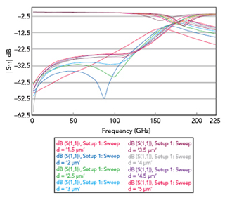
Figure 13 Shows plots of transmission and reflection characteristics of a switch for which the thickness of the second metal layer “d” (e.g., 3230 of Figure 6 varies between 1.5 μm through 5 μm).
Figures 16 and 17 further demonstrate the overall response of the MEMS switch in each of its ON and OFF states, respectively. In Figure 16, when the switch is OFF, and thus not passing the transmitted signal between input and output ports, the reflection characteristics are shown to be just slightly less than 0 dB even at frequencies of up to 130 GHz, the transmission characteristics are between about -20 dB and -15 dB between operating frequencies of about 60 to 130 GHz. In Figure 17, when the switch is ON, and thus passing the transmitted signal between input and output ports, the reflection characteristics are as low as about -73.5 dB at 80 GHz with the transmission characteristics as high as -0.33 dB while the reflection and transmission characteristics at 163 GHz are both about -6.75 dB.

Figure 14 Shows the plot of transmission and reflection properties of a switch for which the thickness of the first metal layer “d1” (e.g., 3210 of Figs. 6 varies between 0.5 μm through 2 μm).

Figure 15 Shows the plot of permittivity extracted from the S-parameters of the composite structure in Figure 6.
The examples of Figures 6 through 17 demonstrate the possibility of incorporating metamaterial structures into a high frequency resistive MEMS switch in order to reduce the effects of stiction.1-2

Figure 16 Response of the MEMS switch.

Figure 17 Response of the MEMS switch.
CONCLUSION
In this article (Part II), the principle of repulsive Casimir force is applied to improve stiction of the resistive contact MEMS switch. This approach can be similarly applied to capacitive contact MEMS switches. As with the resistive switch, a sandwich of metal and dielectric layers used to achieve the desired permittivity interface, such as having a gold layer with infinite permittivity, a dielectric layer with positive but low permittivity and a metamaterial layer with a permittivity in the range of about zero or less. Unlike the example switches here, in the capacitive switch, the metamaterial layer can be used as part of the signal line contact instead of as part of the beam contact and will be covered in Part III (coming in the July issue).
REFERENCES
- Shiban Koul, Chaitanya Mahajan, Ajay Poddar and Ulrich Rohde, “A Microelectromechanical Switch with Metamaterial Contacts, Part I: Concepts and Technology,” Microwave Journal, pp. 82-108, May 2020.
- Shiban Koul, Ajay Poddar and Ulrich Rohde, “Microelectromechanical Switch with Metamaterial Contacts,” US Patent Pub. No. 02161415A1.
- Astrid Lambrecht, “The Casimir Effect: A Force from Nothing,” Physics World, September 2002.
- F. Intravaia and C. Henkel, New Frontiers of Casimir Force, Santa Fe, New Mexico, 2009.
- U. Leonhardt and T. G. Philbin, “Quantum Levitation by Left-Handed Metamaterials,” New J. of Physics, August 2007.
- Mercado et. al., “A Mechanical Approach to Overcome RF MEMS SwitchStiction Problem,” ECTC 2003.
- Ulrich Rohde, Ajay Poddar and Shiban Koul, “MTM: Casimir Effect and Gravity Wave Detection,” APMC 2016.
- Xudong Chen et.al, Robust Method to Retrieve the Constitutive Effective Parameters of Metamaterials, Phy. Rev. E70, 016608, July 2004.
- Chaitanya Mahajan, Design and Analysis of RF MEMS switches (70 GHz to 130 GHz), M.Tech Dissertation, CARE, IIT Delhi, May 2018.