
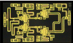
Image courtesy of Mitsubishi Electric
Cadence has released the latest version of the AWR Design Environment®, Version 15 (V15), the first release since the company acquired AWR Corporation from National Instruments. This latest version, available for current customers and evaluators, includes new features, add-on modules and enhancements to the AWR Microwave Office® circuit design software, AWR Visual System Simulator™ (VSS) system design software, AXIEM® 3D planar method of moments and Analyst™3D finite element method electromagnetic (EM) simulators.
New capabilities introduced in V15 help designers address the challenges developing and integrating RFICs, MMICs, device and module packaging and PCB assemblies for 5G, automotive and aerospace and defense applications. These systems increasingly use advanced RF front-end components and antennas that must be designed to achieve spatial and spectral efficiency with minimal power consumption. To meet these needs, the latest release of the AWR Design Environment expands support for power amplifier (PA) and antenna/array design, EM modeling and RF/microwave integration within heterogenous systems.
PAST IS PRESENT...AND FUTURE
Today’s RF technology stems from a long and steady effort among platform integrators, semiconductor manufacturers and electronic design automation (EDA) suppliers. In the late 1980s, the U.S. Department of Defense launched the MIMIC program to develop “affordable, available and broadly applicable” microwave and mmWave subsystems for military systems. The program targeted computer-aided engineering as an essential capability for the development of GaAs MMICs. The MIMIC program and complementary efforts yielded an industrial base for design and semiconductor development, confirmed by technology adoption in military systems and subsequently commercial communications. Cadence, formed in 1988, joined the MIMIC program to develop “smart” microwave libraries, combining electrical models for MMIC components with their physical layouts.
Electronic design has become a complex process, involving an array of analysis, verification and manufacturing tools, reusing design IP to reduce complexity and improve the likelihood of first-pass success. Systems increasingly have embedded radios - Wi-Fi, Bluetooth, cellular or some other standard - and the RF components enabling this wireless connectivity are among the most challenging to design. A holistic approach to the design of the entire system is required.
Cadence is addressing these challenges through the Intelligent System Design™ strategy, delivering its computational software capabilities across all design elements of electronic systems. At the core of this strategy is design excellence, an optimized EDA portfolio of tools with best-in-class RF, microwave and mmWave circuit, system and EM analysis; IP for semiconductor, package and PCB design; and scalable access in the cloud.
THE WIRELESS REVOLUTION WILL BE INTEGRATED
Enabled by wireless, RF will be integrated in an unprecedented number of connected smart devices and systems. Developing these systems requires a significant advance in multi-domain analyses, simulation capacity, design automation and seamless interoperability between RF/microwave EDA and the broader portfolio of mixed-signal IC, PCB, system-in-package and system-on-chip (SoC) design tools. The “more than Moore” pace of electronic design is enabled by technology integration using densely populated, heterogeneous substrates. These tightly stacked components behave as mechanical systems with sophisticated electronics, transporting RF and high speed signals through a complex network of interconnects. To function properly, mixed-technology systems require co-design and co-optimization across multiple domains: RF, analog and digital simulation aided by large-scale EM and thermal analysis, with robust design verification and signoff. AWR’s V15 offers the following features to aid this design process:
Faster EM Analysis of Mixed Technologies
The meshing and solver technologies in the AXIEM EM simulator have been enhanced for speed and capacity to characterize RFICs, MMICs and laminate structures using the latest via meshing technology for “healing” to reduce mesh size (see Figure 1). Complex PCB and SoC components contain manufacturing features that do not impact RF performance, yet they slow EM analysis. Shape pre-processing rules have been expanded to better address large via arrays on user-specified layers inside or outside a specified region. The AXIEM DC solver includes a new sparse symmetric matrix technology that achieves a 10x savings in time and memory.
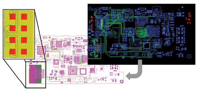
Figure 1 AWR EM analysis of a 28 GHz, 2 x 4 element antenna array on a 5G handset PCB design imported from Cadence Allegro.
Power for the PA Designer
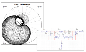
Figure 2 Loop-gain envelope stability analysis enables the stability and margin of each device within an amplifier to be determined.
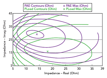
Figure 3 Power and PAE load-pull performance contours on a rectangular grid using V15.
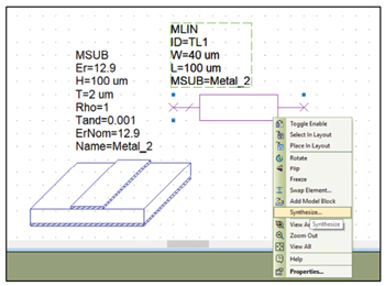
Figure 4 Designers can directly synthesize microstrip, stripline and coplanar waveguide transmission lines from design parameters.
Stability analysis is critical to PA design and optimization. The commonly used K and µ factors cannot detect instabilities in multi-stage amplifiers or devices connected in parallel. Other stability analyses, such as normalized determinate function, overcome these limitations at the cost of computation run time, rendering them too slow for optimization. V15 supports a new loop-gain envelope technique, reducing the simulation time of this rigorous stability analysis from hours to seconds, making it ideal for stability optimization (see Figure 2). Loop-gain envelope stability analysis offers several benefits, the stability and margin of each device within a MMIC amplifier is quantified. Analysis speed is increased by analytically applying the input and output terminations. With this speed improvement, optimization of phase margin for each device within a MMIC is possible, the magnitude of source and load gamma is selectable to quickly determine stability with different loading.
Baseband impedance variation versus frequency in wideband PAs can impact linearity, resulting in intermodulation levels that vary asymmetrically with instantaneous signal bandwidth, behavior associated with baseband memory effects. PA developers have achieved significant improvements in linearity when active, baseband injection architectures such as envelope tracking are employed. Using V15, designers can optimize PA linearity through video band load-pull analysis - along with fourth and fifth harmonic load-pull capability - and plotting performance contours versus load impedance on rectangular graphs (see Figure 3).
Synthesis Accelerates Designs
The characteristic impedance and electrical length of transmission lines - λ/4 impedance transformers, Wilkinson power dividers and combiners, hybrid couplers, filters - are important design parameters for passive RF/microwave circuits. Using V15, designers can directly synthesize these microstrip, stripline or coplanar waveguide structures for a given substrate, based on the desired electrical characteristics (see Figure 4). Similarly, the electrical characteristics can be calculated directly from the physical properties without manually invoking the TX-LINE calculator and inputting the results. The latest synthesis wizard enables users to generate matching networks using components from the Microwave Office supplier library for surface-mount PCB designs or process design kits, extending synthesis to MMIC designs.
SUMMARY
V15 of the Cadence AWR Design Environment brings RF/microwave simulation to Cadence’s portfolio of EDA solutions. New capabilities address stability analysis, video band and fourth and fifth harmonic load-pull and faster harmonic balance. Network synthesis supports optimization using supplier components, single and coupled transmission line synthesis and faster planar EM meshing and solver technology. The Cadence Intelligent System Design strategy envisions a future where electronic design is multi-faceted and relies on multi-physics and a host of design disciplines, with integrated RF, microwave and mmWave content a common factor.
Cadence
El Segundo, Calif.
www.cadence.com