Technical Feature
Performing Transient Analysis on PLL Frequency Synthesizers
A PLL can be considered a subsystem within a larger communications system, so it is appropriate to analyze this type of network with the help of a system-level simulator. The use of flexible behavioral models within the simulator allows only a few parameters to be entered before simulation can be performed. Model detail may also be added as it becomes available to the designer, which permits early prototyping as well as full system characterization.
David Vye
Ansoft Corp.
Pittsburgh, PA
Phase-locked-loop (PLL) frequency synthesizers are used throughout communications systems to provide a stable source of carrier and baseband signals. Since a PLL can be considered a subsystem within a larger communications system, it is appropriate to analyze this type of network with the help of a system-level simulator, such as the Symphony communication system designer within the Serenade software suite. The software utilizes behavioral modeling to simulate the performance of various PLL components and allows designers to examine how component selection can be applied to the design and simulation of a real-world PLL synthesizer. The use of flexible behavioral models means that only a few parameters need to be entered before simulation is possible. Model details may be added as they become available to the designer. This permits early prototyping as well as full system characterization.
Symphony allows engineers of systems and subsystems, such as PLLs, to design at various levels of detail. The simulator easily allows the construction of a PLL synthesizer through the connection of its standard built-in behavioral components, such as a voltage-controlled oscillator (VCO), phase detector, components for loop filter design, reference oscillator and frequency divider. The simulation capability of Symphony performs frequency-domain, time-domain and mixed-mode (time and frequency together) analyses for end-to-end communication system design. Additionally, the software can perform co-simulations through the use of MATLAB1 as well as customized models written in C or C++ language.
Symphony incorporates both functional and electrical behavioral elements. Functional elements do not have electrical representation, such as S-parameters, but rather are defined by a set of signal-processing equations that relate output to input signals. The functional elements are unidirectional, and use a parameter to specify sampling rate for waveform sources or bit rate for binary sources. Electrical elements have an electrical representation, such as S-parameters, in the frequency-domain. Nonlinear electrical elements can be further defined by additional nonlinear figures of merit, such as third-order intercept point, mixer spurious response or 1dB compression point. In addition to having a list of input parameters, many electrical elements may access external (measurement-based) data files. These data files may also include a description of linear data (for instance, S-parameters as a function of input frequency) or nonlinear data (output power and phase as functions of input power).
PLL Basics
PLLs are critical for frequency accuracy in wireless systems, helping to minimize interchannel interference by limiting spectral spreading. In addition, time-division-multiple-access (TDMA) cellular communications systems require synthesizers capable of tuning to a new channel within a small fraction of each time slot. This leads to the need for minimal locking time. The suppression of reference spurious signals and phase noise is also critical in modern digital communications systems, as well as wide tuning range and good frequency stability.
A PLL contains a VCO whose output is fed through a divider circuit back to a phase detector. The phase detector is also fed by a stable reference frequency source, typically a crystal oscillator. The loop filter at the output of the phase detector suppresses reference frequency components and also serves as an integrator. The resulting output signal is then used as a controlling voltage for the VCO, as seen in Figure 1 .
|
|
|
|
Fig. 1 A basic single-loop PLL frequency sythesizer. |
Fig. 2 Linear control model of a PLL in locked state. |
The phase/frequency detector adjusts the voltage presented to the VCO until the feedback frequency matches that of the reference signal. When the system is phase-locked, the VCO is N times that of the reference frequency, where N is the frequency division ratio for the reference oscillator. Changing the value of the divider will cause the phase detector to sense a frequency error. The feedback loop will respond with a correcting voltage. The operating range is set by the maximum frequency of the divider, the division range ratio of the divider and the VCO's tuning range.
A PLL is primarily a nonlinear device because its phase detector is nonlinear. However, when its loop is in a locked condition,2 a PLL can be accurately approximated by a linear control model, shown in Figure 2 . In this case, each of the PLL's components can be described by a linear transfer function. When the loop is closed, the response can be expressed as the ratio of the phases of the VCO and the reference oscillator. As a result, the closed-loop gain, B(s), is equal to the forward gain divided by (1 + the open-loop gain), and the forward gain is the product of the phase detector gain, the VCO gain and the loop filter gain divided by the gain of the divider.
|
|
|
Fig. 3 Bode plot of the open transfer function of a PLL showing the loop bandwidth wp and the phase margin fp . |
A Bode plot of the open-loop gain G(s)H(s) as a function of frequency, as shown in Figure 3 , clearly identifies the loop bandwidth wp , the frequency at which the open-loop has unity gain and the phase margin fp , the difference between the phase at the unity gain point and -180°.
For the loop to be stable, the point of unity gain must occur before the phase reaches 0°. For the best loop performance, the phase margin should be approximately 45°. The loop bandwidth must be carefully chosen with regard to lock time, phase noise, stability and reference-energy suppression.
The design of a PLL loop filter involves several trade-offs, including lock time, noise, stability and reference spurious products. For example, fast lock times are possible with wide loop filter bandwidth, although this will also lead to higher reference spurious products. A wide loop filter bandwidth will also generally improve the close-in phase noise, but may degrade the integrated phase noise. A narrow loop filter bandwidth can reduce reference spurs, but leads to increased lock time and decreased stability.
|
|
|
Fig. 4 Typical second-order filter. |
A PLL's loop filter provides the poles and zeros of the forward gain. A typical second-order filter can be constructed with just a few capacitors and resistors, as shown in Figure 4 . The second-order transfer function is

where the time constants, which determine the pole and zero frequencies of the filter transfer function, are
T2 = R2 C2
and

The values for T1 and T2 depend on the specified loop bandwidth and phase margin.
The phase margin is often specified to be 45° for best performance (for critical damping). The loop bandwidth is specified to achieve the desired overall performance with respect to the lock time, phase noise, stability and reference spurious suppression. Generally, the loop bandwidth is selected as wide as possible for fast lock time, but not too wide as to allow unacceptably high reference spurious levels.
The phase of the open-loop gain as a function of frequency is dependent upon the single pole and zero of the transfer function
f( w) = tan-1 ( wT2 ) - tan-1 ( wT1 ) +180° (3)
The phase margin can then be easily derived by setting the derivative of phase to zero

The values of T1 and T2 can then be determined from

In turn, the filter component values for C1 , R2 and C2 can be obtained from T1 and T2 and the loop bandwidth as

where

For additional rejection of the reference spurious, it may be desirable to add a low pass filter section. The low pass section contributes an additional pole, which must be low enough to provide significant additional reference attenuation and high enough (≥ 5wc ) not to compromise the loop's stability.
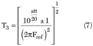
The resulting third-order filter has a time constant for the added low pass section of
T3 = R3 C3
The additional reference attenuation added by the new section is equal to
20log[(2pfref R3 C3 )2 +1]
and the time constant for a given value of additional attenuation is

Using the new filter loop bandwidth of wc , the filter component values can be recalculated where

and the phase-margin degradation caused by R3 C3 is reduced by increasing C1 and C2 and slightly decreasing R2

To demonstrate the effectiveness of the Symphony system-level software in developing practical PLL designs, a 900 MHz PLL was designed with a third-order loop filter. The design features a VCO with tuning sensitivity KVCO = 20 MHz/V, a reference frequency of 200 kHz, attenuation of 20 dB, optimum output frequency (RFopt ) of 900 MHz, a division ratio of RFopt /fref , N = 4500 and optimum phase margin of 45°. The filter is based on a design example from U. Rohde and D. Newkirk.3 The loop bandwidth was chosen as 10 percent of the reference oscillator (wp = 2p • 20 kHz = 1.256 • 105 ).
|
|
|
Fig. 5 A 900 MHz PLL example in Symphony using behavioral models and signal probes. |
A similar 900 MHz PLL is also available as an example in the Symphony software package. The software contains all of the components needed to create the PLL, including the VCO, divider, reference oscillator, second-order loop filter and phase detector. The reference oscillator has a sinusoidal output that must be sampled in the time-domain. The designer must specify a sample rate that is at least twice the maximum frequency swing of the VCO according to Nyquist criteria, as well as the number of samples to be used, which can be determined by the product of the sample rate and the estimated lock time. Figure 5 shows the 900 MHz PLL example.
A designer must also specify the frequency, power and phase noise of the reference oscillator. According to Leeson's model,4 the power spectral density of the reference oscillator's random phase noise is

where
fm = frequency offset
flo = center frequency
Plo = average power at oscillator output
fc = flicker noise frequency
Qload = loaded quality factor (Q) of the reference oscillator
The frequency offsets F1 and F2 define the behavior of the desired oscillator type (Figure 6 ), where type 0 is a low Q oscillator and type 1 is a high Q oscillator. For a low loaded Q, F1 and F2 correspond to fc and flo /2Qload , respectively, while for a high loaded Q, F1 and F2 correspond to flo /2Qload and fc , respectively. The frequency response of the reference oscillator can be broken down into three regions: (1) the region near the carrier, where fm < F1; (2) the region far from the carrier, where F1 < fm < F2; and (3) the white noise region, where fm ≥F2. Regions 1 and 2 are represented in the frequency-domain with 8192 frequency points each. Region 1 typically requires much finer frequency resolution than region 2. Region 3 is modeled as an additive white Gaussian noise (AWGN) process. The total random phase noise process is simply the sum of the contributions from each region. Since the sampling frequency of the generated phase noise process is less than the actual output sampling frequency, linear interpolation is applied on the generated phase noise process in the time-domain to ensure that it has the same sampling rate as the output signal.
The next PLL component to model is the frequency divider. The frequency divider converts the input signal at a given frequency to a new frequency based on the ratio of the frequency divider, N. If the reference frequency is 200 kHz and the frequency of the free-running VCO is 905 MHz, then N = 900 MHz ÷ 200 kHz = 4500. This results in a difference of 905 - 900 MHz or a 5 MHz frequency jump to achieve a locked condition. The final tuning voltage after achieving lock can be found from

Following this, the loop filter can be specified in Symphony in a number of different ways. The loop filter can be specified as a collection of functional elements, such as poles and zeros, as lumped-element circuits or as S-parameter data. A complex multiplier handles the phase detector in this 900 MHz design example. The signals from the reference oscillator and the divided-down VCO signals are fed to the inputs of the multiplier. The output of the multiplier is the product of these two signals. Two types of multipliers are available in Symphony, for both high side and low side multiplication, respectively. As an alternative to the complex multiplier, a charge-pump circuit can be used as a phase detector. A phase-frequency detector, for example, can be created from a D-type flip-flop device.
Once a PLL subsystem has been designed and created in software, software probes are used to view the operation of the system. A variety of different probes are available for this purpose, including signal probes (which measure voltages at functional nodes), signal-to-noise-ratio (SNR) probes, bit-error-rate (BER) probes, adjacent-channel-power-ratio (ACPR) probes, frequency trajectory probes, power probes and voltage probes (which measure voltages at electrical nodes). In the example PLL design, signal probes have been placed after the phase detector and the loop filter in order to view the phase-error signal and the input to the VCO. The PLL lock time can be deduced by viewing the instantaneous frequency as a function of simulation time using the frequency trajectory probe (Figure 7 ).
|
|
|
Fig. 7 PLL settling time display using a frequency trajectory probe. |
Simulation Results
Simulated performance results are shown via time-domain signal probes. These probes show the signal after the multiplier and from the phase detector. This signal is then used to control the VCO. This signal contains all the mixing products of the divided-down VCO signal and the reference oscillator signal. The amplitude of the envelope shows the difference of these signals. A close-up plot of the trace shows the sum frequency (fref + fVCO /N). The change in frequency as the PLL locks is seen by the change in the period from the beginning of the trace and back. In this design, the loop filter and integrator have effectively reduced the level of reference spurs.
Alternately, the probe response could have been viewed in the frequency (spectral) domain. The center peak actually contains two peaks, ±(fref + fVCO /N). In this case, the frequency trajectory probe has been placed after the VCO to indicate the actual locking time, which was determined to be 300 ms.
|
|
|
Fig. 8 A 900 MHz PLL synthesizer based on an active loop filter design. |
The 900 MHz PLL can also be realized with an active filter rather than the passive lumped-element filter, as shown in Figure 8 . The active (second-order-type) filter can be constructed with a finite-gain operational amplifier, lumped electrical elements and an integrator (a functional element in the software). Because the op amp has finite-gain, it does not behave as a true integrator (with infinite gain at 0 Hz). Instead, the active filter has a low frequency pole and actually functions as a second-order loop. Because the loop filter has one low frequency pole and a second pole at a much higher frequency, the simulation time will be extremely long and memory-intensive due to the long time-domain impulse response required for the low frequency pole and the small time step required for the high frequency pole. To accelerate the simulation time, the filter should be converted to a single-order type with separate integrator.
Conclusion
A practical PLL design utilizing system-level simulation and electrical/functional behavioral models has been demonstrated. Equations for specifying filter characteristics were derived and applied to the design. The resulting 900 MHz PLL was determined to have a 300 ms locking time given a 905 MHz free-running oscillation frequency. Further analysis could be applied to determine output power and phase noise.
References
1. Available from MATHWORKS, Natick, MA.
2. D. Byrd, C. Davis and W.O. Keese, "A Fast Locking Scheme for Frequency Synthesizers," National Semiconductor Application Note 1000 , July 1995.
3. U. Rohde and D. Newkirk, RF/Microwave Circuit Design for Wireless Applications , John Wiley & Sons, New York, NY, 2000.
4. D.B. Leeson, "A Simple Model of Feedback Oscillator Noise Spectrum," Proceedings of the IEEE , 54, 1966, pp. 329-330.
David Vye is the product marketing manager for Ansoft Corp.'s high frequency circuit/system design and simulation tools. He is a 1984 graduate of the University of Massachusetts at Dartmouth, with a concentration in microwave engineering. He first joined M/A-COM's Advanced Semiconductor Operations, developing test and device characterization methods for power GaAs MESFET technology, as well as MMIC design. In 1987, he joined Raytheon's research division, where he was responsible for IMPATT diode transmitter development for a number of millimeter-wave applications. Between the years 1994 to 1998, he was a member of the design staff at Raytheon's Advance Device Center. His responsibilities included circuit development (MMIC) and device modeling for AlInAs/GaInAsInP PHEMT and GaAs HBT technologies. He joined Ansoft in 1998.


