
Technical Feature
An Embedded MOS Model 9 for CMOS RF Circuit Design
This article presents an n-channel MOS transistor model for the simulation of CMOS RF circuits in the gigahertz range. This model is based on a MOS model 9 (MM9) compact transistor model, embedded in a network describing device parasitics. The parasitics network consists of six resistors, five capacitors and two JUNCAP diode models. Methods for device characterization and determination of the parasitics are presented. A model, developed for a 0.25 mm CMOS technology, shows good accuracy in the measured frequency range up to 12 GHz and over a wide bias range. By applying simple rules for the scaling of parasitics and a unit transistor layout approach, the model also shows excellent scalability with respect to device width. It also predicts intermodulation products with fair accuracy.
Christian Rye Iversen
Siemens Mobile Phones A/S
Pandrup, Denmark
With the advent of sub-micron silicon CMOS technologies, gigahertz RF circuits are now realizable in standard CMOS processes.1,2,3 Although CMOS is notorious for its inferior performance as an RFIC technology, it certainly has some very interesting properties for realizing competitive radio solutions for the wireless communications industry. One of the major advantages of CMOS RF circuits is that they may be integrated on-chip with large-scale digital circuits, such as digital signal processors and CPUs. CMOS is thus the technology of choice for compact single-chip radio transceivers that include both RF, analog and digital processing. Another very important advantage of CMOS is that it has the lowest cost per mm2, while it also enjoys the major part of the semiconductor industry investments.
Requirements for simultaneous improvements in cost, power consumption, size and performance compels today's RF circuit designers to work with much greater refinement. Due to the generally lower performance of both active and passive devices, CMOS RF circuit designers are forced to work even harder to achieve a given level of performance. One of the obstacles in designing RF circuits in CMOS is the lack of adequate models that predict MOSFET device behavior at gigahertz frequencies. Although measured device S-parameters can be used to some extent for the design of some circuits such as LNAs, they require extensive data from numerous bias conditions and device geometries, and they are quite cumbersome since they do not combine DC and RF simulations. Furthermore, S-parameters cannot predict nonlinear parameters such as compression and intercept points. Other circuits that rely on nonlinear phenomena, such as oscillators and mixers, cannot be properly designed using only small-signal data. Hence, a compact MOSFET model, valid for a broad range of bias conditions and operating frequencies, is desirable.
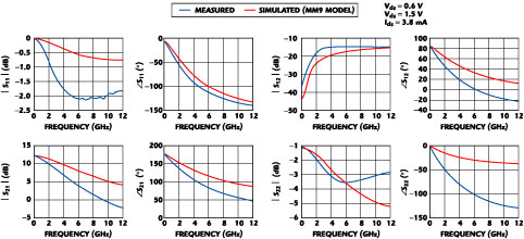
Fig. 1 Comparison between measured and simulated S-parameters for a 400 x 0.25 mm NMOST.
For low frequency circuit design, compact MOS models such as MM94 , BSIM3v35 and EKV6 are widely accepted. However, applying these models at gigahertz frequencies without parasitic effects gives inaccurate results.7 This is clearly illustrated in Figure 1 , which shows a comparison between measured and modeled S-parameters for a 400 x 0.25 mm NMOST (n-channel MOS transistor) in a standard digital 0.25 mm CMOS technology (0.2 mm effective gate length). The model used is an MM9, developed by Philips, with no extrinsic parasitics. As can be seen, application of the MM9 without parasitics is limited to frequencies below a few hundred megahertz.
This article describes a simple extension of the compact MM9 model with a network of parasitic elements. The extended model enables accurate prediction of NMOST S-parameters over a wide bias range and for frequencies up to 12 GHz. The device parasitics are determined from S-parameter measurements on a 400 x 0.25 mm NMOST reference device in both common source (CS) and common gate (CG) configurations. It is also shown that by employing a unit transistor layout approach for scalability of device parasitics, the model can be used over a wide range of device widths. Test results that verify the model performance over bias and device width are given, and the model is also evaluated for predicting second- and third-order intermodulation products.
MOS Transistor Parasitics
The considerable discrepancy between measured and modeled S-parameters is due to fact that MM9 models only the intrinsic device, and does not include the parasitics associated with the actual device. At lower frequencies these parasitics have only a negligible effect, whereas they are very important at gigahertz frequencies. Some insight to the parasitics associated with the NMOST device can be gained by inspecting the transistor cross-section illustrated in Figure 2 .
|
|
|
|
Fig. 2 NMOST cross-section for a single finger transistor. |
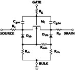
Fig. 3 MOS transistor equivalent circuit proposed by C. Enz.7 |
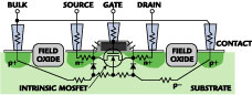
The connections to the intrinsic device contribute series resistances to all four terminals of the NMOST. The source and drain terminals have series resistances contributed by the contacts and the n+ diffusions connecting to the intrinsic source and drain terminals. The gate series resistance is due to the contact and the n+ polysilicon gate material. From the bulk connections outside the actual transistor, there is also considerable series resistance to the intrinsic bulk terminal, mainly contributed by the resistive p-substrate. The source-bulk and drain-bulk diodes are reverse biased in normal operation but contribute a capacitive coupling to the resistive substrate. In modern sub-micron CMOS technologies, the gate terminal overlaps the source and drain regions resulting in gate-source and gate-drain overlap capacitances. The metal used to interconnect multiple fingers of a transistor is not shown. It also contributes a terminal series resistance and inter-terminal parasitic capacitances. The parasitics contributed by interconnect metal are bias independent, whereas the other parasitics are potentially bias dependent.
In a compromise between accuracy and complexity, the NMOST equivalent circuit model shown in Figure 3 has been proposed for RF circuit simulations by C. Enz, et al.7 It contains the compact transistor model Mi , the terminal resistances Rg , Rd and Rs , the simplified substrate resistor network Rsb , Rdb and Rdsb , the source-bulk and drain-bulk diodes Dsb and Ddb , and the parasitic gate-source and gate-drain capacitors Cgse and Cgde .
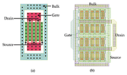
Fig. 4 NMOST transistor layout; (a) 20 x 0.25 mm unit transistor and (b) a 450 x 0.25 mm
transistor built from 20 unit transistors in parallel.
MOS Transistor Layout for Scalability of Parasitics
One of the important features of an RF MOS transistor model is that it provides scalability with respect to device width. To accomplish this in a simple manner, it is necessary that the device parasitics scale with device width. An effective technique to realize this is to use a unit transistor approach.8 For example, all the devices used in this work are created by using a 20 x 0.25 mm unit transistor, which has four fingers, each of 5 mm width. Larger transistor widths are then formed by placing a number of unit transistors in parallel, as shown in Figure 4 , where 20 unit transistors are used to obtain a 400 x 0.25 mm transistor. As previously reported,8 this technique has proven to give good scalability of the extrinsic parasitics. Therefore, the following simple scaling rules can be applied to estimate the parasitics for devices with different widths.

where
Rx,W = parasitic resistance for a device of width W
Rx,Wref = corresponding parasitic resistance for a reference device of width Wref
Nunit,W = number of unit cell transistors to form a device of width W
Nunit,Wref = number of unit cell transistors to form a device of width Wref
For capacitive parasitics
Cx,W = parasitic capacitance for a device of width W
Cx,Wref = corresponding parasitic capacitance for a reference device of width Wref
NMOST Model Development
The development of a NMOST model for a 0.25 mm standard digital CMOS process is described in this section. It is based on a 400 x 0.25 mm reference device. The reference device width has been chosen to be in the range of a typical RF NMOST used in the low gigahertz range. As the reference device is laid out, using the unit transistor approach, this model should be scalable to other device widths. The device gate length is restricted, however, to the minimum 0.25 mm, since this is an obvious choice for optimum device performance at RF. The focus has been on the strong inversion and saturation region of operation, as the model was originally developed for LNA design. The intrinsic device is modeled with MM9, for which the CMOS foundry supplies a set of parameters. In addition to these parameters, MM9 requires the gate width, gate length and device temperature. The source-bulk and drain-bulk diodes have been modeled using a JUNCAP model also developed by Philips.4 The parameters of this model are also supplied by the foundry. As mentioned above, the parasitics of the NMOST are potentially bias dependent. However, as the goal has been a simple model extension, they have been assumed to be bias independent, although this may limit both accuracy and applicable bias range.
|
Table 1 | ||||||||
|
W |
Vds , Ids |
es |
W |
Vds , Ids |
es |
W |
Vds , Ids |
es |
|
400 |
1.0 |
0.10 |
200 |
1.0 |
0.13 |
560 |
1.0 |
0.11 |
|
2.0 |
0.23 |
2.0 |
0.21 |
2.0 |
0.24 | |||
|
1.5 |
0.65 |
1.5 |
0.45 |
1.5 |
0.40 | |||
|
1.5 |
0.07 |
1.5 |
0.05 |
1.5 |
0.10 | |||
Device Characterization
A key issue in developing an NMOST model for RF circuit design is that the NMOST is a four-terminal device. Device characterization at both DC and RF has yet to take this into account. In CMOS RFIC design the resistive substrate is usually well grounded, using an extensive number of substrate pick-ups to avoid unintentional coupling. The transistor bulk terminal can therefore be assumed connected to ground, whereas the other three terminals can be connected in numerous configurations depending on the circuit. This basic fact is often overlooked in NMOST modeling, and both the source and bulk terminals are connected to ground. Unfortunately, this common source configuration is rarely used in CMOS RFIC design, and a model restricted to only common source is thus of limited use.
A full small-signal RF characterization of the NMOST can be done by measuring three-port S-parameters. However, with access to only two-port vector network analyzer equipment, three-port measurements are very cumbersome and error-prone, especially over many bias points. In order to avoid three-port measurements, the RF characterization has, in this case, been done by two-port measurements in both CS and CG configuration. These two measurement configurations are shown in Figure 5 .
|
|
|
|
Fig. 5 Characterization of the four-terminal MOS transistor using both common source (a) and common gate (b) configurations. |
Fig. 6 Modeled and measured zero-back bias DC characteristics. |


In the CG configuration, the gate is RF short-circuited to ground/bulk using a 10 pF MOS capacitor. Since the MOS capacitor does not present a perfect short circuit at the gate, it has been characterized separately by measuring S-parameters as a function of bias. These S-parameters are then used during characterization of the NMOST. In both configurations, the devices have been placed in a shielded measurement fixture for accurate on-wafer CMOS measurements.9 The measured S-parameters are de-embedded using a four step de-embedding method.10 Preferably, the fixturized CS and CG devices should be placed close to each other on the same die to improve device matching.
An important concern, when developing an RF transistor model by embedding a compact model in a network of parasitics, is that the compact model fits the DC characteristics of the device that is used in the RF measurements. To verify this, an initial DC characterization is required, both in the zero-back bias condition (source-to-bulk voltage VSB ≠ 0 V, CS configuration) and for different back bias voltages (VSB ≠ 0 V, CG configuration). Preferably, DC measurements should be carried out on many devices spanning several wafers in order to select a typical device. If a noticeable difference between the measured and modeled DC characteristics is observed, the parameters of the compact MOS model must be adjusted or re-extracted. If the difference in the DC characteristics is owed to natural device spread and not poorly extracted parameters, the parameters of the compact MOS model should be changed back to their original values after extraction of the parasitics.

Fig. 7 Modeled and measured S-parameters at the Vds = 1.5 V, Ids = 17.6 mA bias point in CS configuration.
In this case, the most typical device was selected from measurements on 10 different dies, although from the same wafer. By comparing the measured DC characteristics with the model, it was found that five parameters of the MM9 needed to be modified to give an acceptable fit. The modified MM9 parameters are VTOR (threshold voltage in zero-back bias), bsq (gain factor of an infinite square transistor), x1R (weak inversion correction factor), VSBXR (transition voltage for dual k factor model) and KR (high back bias body factor). The measured and modeled zero-back bias DC characteristics are shown in Figure 6 .
Determination of Parasitic Elements
The determination of the parasitic elements is based on measured S-parameters in both CS and CG configuration. Optimization is used to obtain optimum fit between the measured and simulated S-parameters over a number of bias conditions. For this purpose, an error function expressing the difference between the measured and simulated S-parameters is formulated as
where
Nfreq = number of frequencies
Nbias = number of bias points
Sij,model = modeled two-port S-parameters
Sij,measured = measured two-port S-parameters
|
|
|
Fig. 8 MM9RF, NMOST equivalent circuit. |
To determine the parasitics of the model shown previously, eighteen sets of measured S-parameters for different bias points were used. Nine were measured in the CS configuration and nine in the CG configuration. The optimization was done using Advanced Design System (ADS) by Agilent Technologies. To ease convergence, a first optimization was done with only one central bias point in CS and one central bias point in CG using a random optimizer. Next, the full number of bias points was used, and a gradient optimizer was used to fine tune the parasitics.
With the proposed model, an error function value of es = 5.3 percent was obtained after a thorough optimization. To illustrate the quality of this fit, a comparison between measured and modeled S-parameters for one bias point in the CS configuration is shown in Figure 7 . This bias point has been chosen for illustration since it has an error of es = 5.0 percent, which is close to the value averaged over the 18 bias points. Although the fit is improved considerably compared to that from the compact model, it is still not found satisfactory.
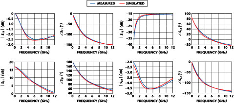
Fig. 9 MM9RF modeled and measured S-parameters at the Vds = 2.1 V, Ids = 10.7 mA bias point in CS configuration.
The MM9RF Model
To improve the fit, an extension of the original model was necessary. It was found that the model needed three additional capacitors Cdse , Csbe , and Cdbe , as shown in Figure 8 . This model is referred to as MM9RF, and, by optimizing, the error function value was reduced to only 0.21 percent. Compared to the original model, this is a reduction of the error function value by approximately a factor of 25. Shown in Figures 9 and 10 are measured and modeled S-parameters for CS and CG configurations, respectively. The selected bias points have error function values close to the average 0.21 percent. As shown, an excellent fit is obtained. The parasitic values for the 400 x 0.25 mm reference device are Rg = 0.63 W, Rs = 80.0 mW, Rd = 80.0 mW, Rsb = 15.2 W, Rdb = 20.7 W, Rdsb = 289.0 W, Csbe = 124.0 fF, Cdbe = 36.6 fF, Cgse = 10.8 fF, Cgde = 99.8 fF and Cdse = 174.0 fF.

Fig. 10 MM9RF modeled and measured S-parameters at the Vds =0.9 V, Ids = 2.8 mA, Vsb = 0 V bias point in CG configuration.
Evaluation of MM9RF Performance
|
|
|
Fig. 11 Error function evaluated for 40 bias points in the CS configuration (Vsb = 0 V). |
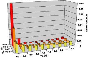
To evaluate the performance of the developed MM9RF model several tests were carried out. The error function values evaluated over a larger bias range in CS configuration show a very good fit over the examined bias range, except for VDS = 0.3 V. Examination of the measured and modeled S-parameters has shown that the principal cause of errors at VDS = 0.3 V is the failure of the original model (MM9) to represent correctly the DC characteristics in this region. Tests carried out for the CG configuration and with back bias (VSB ≠ 0 V) show a similar level of accuracy, as seen in Figure 11 .
If the scaling rule of Equation 1 holds, the MM9RF model should be able to predict the S-parameters for devices with widths different from the 400 mm used in the model development. In order to test this assumption, measured and modeled S-parameters were compared for a 200 x 0.25 mm and a 560 x 0.25 mm device in the CS configuration. The results are listed in Table 1 . As seen, the error function values for both the 200 x 0.25 mm and the 560 x 0.25 mm devices are comparable to those of the 400 x 0.25 mm device used for the model development. The modeled and measured S-parameters for a 200 x 0.25 mm device are compared in Figure 12 .
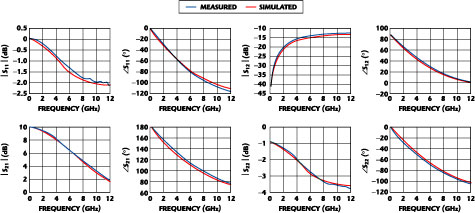
Fig. 12 MM9RF modeled and measured S-parameters for 200 x 0.25 mm NMOST biased at Vds = 1.0 V, Ids = 4.0 mA in CS configuration.
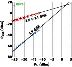
Another very important feature of a MOS transistor model for RF circuit design is its ability to predict nonlinear phenomena such as intermodulation distortion. As a test, both second- and third-order intermodulation have been measured and simulated. In both tests, a 400 x 0.25 mm device biased at VDS = 1.5 V and IDS = 6.1 mA was used. The oIP2 was determined by applying a 1 GHz input signal and measuring the 2 GHz second harmonic. The oIP2 determined by measurements is 18.4 dBm, whereas the simulated value is 17.7 dBm. By applying a two-tone test signal at 2.0 and 2.1 GHz, and measuring the third-order 1.9 GHz intermodulation product, the third-order intercept point referred at the output (oIP3) was measured to be 13.7 dBm. By simulating the same excitation and using harmonic balance in ADS, an oIP3 of 15.4 dBm was obtained. The simulated result is only 1.7 dB higher than the measured result, a good agreement for this parameter. Figure 13 shows the measured oIP3 results.
Conclusion
|
|
|
Fig. 13 Measured third-order intermodulation product. |
An NMOST model applicable for simulation of CMOS RFICs in the gigahertz range is presented. The model is based on a compact MM9 model embedded in a network of parasitics. It is shown that the pure MM9 fails to predict device behavior above a few hundred megahertz. However, with the proposed extension, the model shows excellent accuracy up to 12 GHz and over a wide bias range. The parasitics consist of two JUNCAP models, six resistors and five capacitors. The resistors and capacitors are bias independent. By using a unit transistor approach in MOS transistor layout and simple scaling rules for the parasitics, the model has shown good scalability with respect to device width. The model shows fair accuracy in predicting nonlinear parameters such as oIP3 and oIP2.
References
1. T.H. Lee and S. Wong, "CMOS RF Integrated Circuits at 5 GHz and Beyond," Proceedings of the IEEE , Vol. 88, No. 10, Oct. 2000.
2. A. Rofougaran, G. Chang, J.J. Rael, J.Y.C. Chang, M. Rofougaran, P.J. Chang, M. Djafari, M.K. Ku, E.W. Roth, A.A. Abidi and H. Samueli, "A Single-chip 900 MHz Spread-spectrum Wireless Transceiver in 1 mm CMOS," IEEE Journal of Solid-state Circuits , Vol. 33, No. 4, Apr. 1998, pp. 515-547.
3. Silicon Laboratories Aero GSM Transceiver. See http://www.silabs.com.
4. MOS Model 9 and JUNCAP documentation [online] available at http://www.semiconductors.philips.com/Philips_Models/.
5. Y. Cheng, M. Jeng, Z. Liu, J. Huang, M. Chan, K. Chen, P. Ko and C. Hu, "A Physical and Scalable I-V Model in BSIM3v3 for Analog/Digital Circuit Simulation," IEEE Transactions on Electron Devices , Vol. 44, No. 2, Feb. 1997, pp. 277-287.
6. C.C. Enz, F. Krummenacher and E.A. Vittoz, "An Analytical MOS Transistor Model Valid in All Regions of Operation and Dedicated to Low Voltage and Low Current Applications," Special Issue of the Analog Integrated Circuits and Signal Processing Journal on Low Voltage and Low Power Design , Vol. 8, Jul. 1995, pp. 83-114.
7. C. Enz and Y. Cheng, "MOS Transistor Modeling for RF IC Design," IEEE Transactions on Solid-state Circuits , Vol. 35, No. 2, Feb. 2000, pp. 186-201.
8. T.E. Kolding, "Consistent Layout Techniques for Successful RF CMOS Design," Proceedings of Workshop on New Technologies for RF Circuits, Microwave Engineering Europe , Bracknell, UK, Mar. 2000, pp. 46-56.
9. T.E. Kolding, O.K. Jensen and T. Larsen, "Ground-shielded Measuring Technique for Accurate On-wafer Characterization of RF CMOS Devices," Proceedings of IEEE International Conference on Microelectronic Test Structures (ICMTS) , Monterey, CA, Mar. 2000, pp. 246-251.
10. T.E. Kolding, "A Four-step Method for De-embedding Gigahertz On-wafer CMOS Measurements," IEEE Transactions on Electron Devices , Vol. 47, No. 4, Apr. 2000, pp. 734-740.