Technical Feature
Aluminum Nitride vs. Beryllium Oxide for High Power Resistor Products
Michael Kettner, Patrick Biebersmith, Nelson Roldan And Balram K. Sharma
Florida RF Labs Inc.
Stuart, FL
For the past few decades, beryllium oxide (BeO) has been the main substrate material used for RF resistors and terminations for high power applications. Although BeO is well suited for high power applications in the electronics industry, its dust particles are toxic; if BeO particles are inhaled, they may cause berylliosis, an inflammation of the lungs. Due to emerging health and safety regulations worldwide, industries are limiting the use of BeO as a ceramic substrate material. Consequently, the electronics industry is searching for environmentally-friendly substrate material to replace BeO. The early development of aluminum nitride (AlN) took place in the 1960s for applications in ceramic packages. AlN boasts a thermal conductivity far superior to that of alumina and a dielectric constant no more than that of alumina. AlN's full potential for electronic applications was not fully realized at that time.
Properties of AlN and BeO
After extensive research and development, along with improvements in thermal conductivity, AlN has emerged as an alternative to BeO for substrate material. Although it does not serve as a 100 percent direct replacement for BeO, it is non-toxic, safe to handle and has a thermal conductivity much higher than alumina (Al2 O3 ) and approaching that of BeO. Table 1 details the electrical and physical properties of AlN, BeO and Al2 O3 . AlN's dielectric constant of 8.9 is higher than that of BeO, which is of concern to circuit designers since it causes high shunt capacitance. Therefore, design rules established for BeO cannot be used for AlN substrates. It is possible to introduce tuning circuits on designs with AlN devices in order to overcome the effect of additional capacitance. A design guideline for tuning out the capacitance is included in the next section. Thermal analysis data available on AlN allows designers to use this substrate material for high power microwave applications. In 1996, the potential of AlN for its resistors and terminations was first realized.
|
Table 1 | |||
|
Property |
AlN |
BeO |
Al2 O3 |
|
Dielectric constant (1 MHz @ RT) |
8.9 |
6.7 |
9.8 |
|
Dielectric loss (1 MHz @ RT) |
0.0001 |
0.0003 |
0.0002 |
|
Electrical resistivity (Ohm-cm) |
< 1014 |
< 1014 |
< 1014 |
|
Thermal conductivity (W/m K) |
170-190 |
260 |
36 |
|
Coefficient of thermal expansion (ppm/°C) |
4.6 |
8.5 |
8.2 |
|
Density (g/cm3 ) |
3.30 |
3.85 |
2.89 |
|
Bending strength (mPa) |
290 |
230 |
380 |
|
Hardness (knoop) (GPa) |
11.8 |
9.8 |
14.1 |
|
Young's modulus (GPa) |
331 |
345 |
372 |
Standard thick film paste systems developed for Al2 O3 and BeO ceramics some decades ago were found to be unsuitable on AlN ceramic material. Thick film paste manufacturers had to invest resources to develop new thick film pastes and processes compatible with AlN. Whether using AlN, BeO or Al2 O3 , the key to a successful thick film paste system centers on the long-term adhesion reliability of the fired thick film to the ceramic substrate. In the case of AlN, the surface must be properly prepared before thick film paste can be applied. This would normally involve lapping the surface or instituting a cleaning process utilizing a special solvent. To compare the surface finish between BeO and AlN, surface scans using the 3D Surface Scan Profiler KLA-Tencor P-11 were performed. Figure 1 details the surface profile of an "as fired" 10 to 15 min BeO, which appears non-uniform, rough and less dense with low surface defects. Similarly, Figure 2 shows the surface profile of a 32 min lapped AlN, which appears uniform, less rough and highly dense. Table 2 compares values of the 3D scan roughness of BeO and AlN.
|
|
|
|
Fig. 1 Surface scan of a BeO sample. |
Fig. 2 Surface scan of an AlN sample. |
Surface finishes like this are acceptable for thick film but not for thin film applications. Any surface defects introduced during the lapping process could seriously degrade the performance of the component. The effect of surface roughness on the resistors produces variation in resistance values across the surface of the substrate. For thin film applications, surface finishes of 2 to 6 min are suitable, which minimize any resistance variation across the surface. This level of surface finish is achieved by polishing the rough surface until the desired surface finish is attained.
Unlike BeO, AlN requires the selection of a suitable vendor and then tuning the fabrication process to qualify the substrates. Since different vendors produce variations in composition and surface finish, selecting the correct vendor is important. A suitable vendor also reduces inconsistencies between batches.
|
Table 2 | ||
|
Sample |
Sq (RMS Roughness) |
Sa (AVG Roughness) |
|
BeO |
4489.5 |
3433.2 |
|
AlN |
7741.1 |
6156.6 |
Thin film technology has been successfully applied to AlN ceramic substrates for fabrication of RF resistors and terminations for high power applications. Since an AlN surface, whether for thin or thick film applications, decomposes to amorphous aluminum hydroxide when in contact with water at elevated temperature, it is important to exercise great control when carrying out thin film processing. AlN reacts with cleaning solutions containing ammonia. The ammonia will etch the substrate and produce a porous surface finish. All these reactions lead to poor adhesion between the film and the substrate, and also create a variation in resistance values across the substrate.
Similarly, potential reliability problems can be foreseen in AlN high power resistive components when operated at and above 100°C in a humid condition. To overcome this problem, the film element is protected against moisture and damage due to handling during processing with SiO2 or polyimide coating.
Designing with AlN
Regardless of which type of substrate material is being used, a design must contend with the capacitive property of the material. The capacitance of BeO and AlN can be tuned out by using a matching network to counteract the capacitance. A 150 W tab and cover termination will be used as a design example that reveals the capacitance of the material and demonstrates how using a matching network can neutralize the effect of the capacitance.
The design specifics are a 0.250" x 0.375" AlN substrate, nickel chromium thin film, SWR < 1.06, frequency range of DC to 2.0 GHz and 150 W power dissipation. Starting the design requires determining the film area using the formula for steady state heat flow as

where
T = temperature of film (°C)
TA = ambient temperature (°C)
P = power dissipated (W)
D = substrate thickness (m)
A = film area (m2 )
k = thermal conductivity (W/m°C)
The substrate thickness is 40 mil and the ambient temperature is assumed to be 25°C. The maximum film temperature will be limited to 125°C. The thermal conductivity of AlN at 200°C is 130 W/m°C. Solving Equation 1 for A yields a film area of 24,226 mil2 . A more conservative formula using the power density of the substrate material can also be used to calculate the area

where
PD = power density (W/m2 )
P = device power (W)
A = area of film (m2 )
The power density for AlN can be from 619 to 883 W/m2 depending on the layout and process of the power dissipating elements. After finding the film area, some equivalent circuit component values can be found for a square film pattern. Using the area found with Equation 1, the line width and length must be 155.6 mil.
|
|
|
|
Fig. 3 Capacitance vs. frequency of 150 W termination. |
Fig. 4 Smith chart impedance of the untuned circuit. |
Finding the equivalent circuit components requires the use of standard microstrip formulas for a lossless transmission line. Using the calculated width of 155.6 mil and a substrate thickness of 40 mils, the equation yields a characteristic impedance of 26.53 W and a phase velocity of 5.32 x 10⁹ in/s. With these values calculated, the lumped circuit per unit length inductance of 7.687 x 10⁻¹⁰ H and the capacitance of 3.708 x 10⁻¹³ F were found. Microwave Office was used to create the following data plots with the previous calculated values. Figure 3 shows capacitance vs. frequency for the untuned circuit. Figure 4 is the Smith chart plot of the un-tuned impedance.
|
|
|
|
|
Fig. 5 The untuned circuit. |
Fig. 6 Tuned circuit capacitance vs. frequency of the 150 W termination. |
Fig. 7 Smith chart impedance of the tuned circuit. |
As the data indicate, the device starts out almost purely capacitive and, as the frequency increases, some inductance begins to appear. The layout of the untuned part is shown in Figure 5 . The next step in the design is to calculate an impedance matching scheme that eliminates the capacitance. By using the complex impedance of the untuned design at 2 GHz reactance, values can be found that effectively eliminate most, if not all, of the capacitance. A simple matching network can be used to calculate the components required to make the device 50 W. Figure 6 displays the new values for the capacitance over the entire frequency range after the matching network was applied. Note how the capacitance decreases as the frequency nears its limit. The graph also shows the significant change in the capacitance from the addition of the matching network. Figure 7 is the new Smith chart plot of the tuned circuit. The maximum SWR was changed from 1.70 to 1.04 by adding the matched network. The deviation from a perfect match is due to insufficient precision in the matching components. The new layout with tuning is shown in Figure 8 .
The final step of the design process is to include the realization of the appropriate lumped elements by distributed approximations. In general, a length-to-width ratio of greater than 1 will realize inductors and a length-to-width ratio of less than 1 will realize capacitors. Another consideration is to verify that the manufacturing process is capable of building the desired dimensions for the realization of the circuit components.
|
|
|
|
Fig. 8 The tuned circuit. |
Fig. 9 Tab pull test arrangement. |
Experimental Data
Samples were manufactured and assembled in accordance with the company's procedures. For these tests, chips were prepared using tin lead plated tabs soldered to the pads using Sn62 solder, and Ni plated flange soldered to the chip using pre-form Sn62 solder. The following tests were carried out using a Chatillion force gauge in accordance with MIL-STD-883 specification. The data obtained was analyzed and tabulated as follows.
A horizontal force was applied to the tab until it was pulled free of the pad. The pull test was conducted as shown in Figure 9 with a cover on the top of the element since many of these components are supplied to the users with a cover attached to the base chip. Table 3 lists the pull test results.
|
|
| ||||||||||||||||||||||||||||||||||||
Horizontal force was applied to the chip soldered to the heat sink as in Figure 10 . The applied force was increased to a point that caused the chip to shear off the heat sink or in some case cracked the chip without any damage to the solder joint. Table 4 lists the shear test results.
The endurance test data in Figures 11 and 12 show that resistors on AlN and BeO tend to stabilize to a value that is within specified tolerance for the resistors. Film temperature measured on the cover during the endurance test at 150 W reached 190°C for AlN and 184°C for BeO. As expected, BeO has maintained a lower temperature than AlN due to its high thermal conductivity.
|
|
|
|
|
Fig. 10 Stress test arrangement. |
Fig. 11 Endurance test on the termination on AlN substrate. |
Fig. 12 Endurance test on the termination on BeO substrate. |
Thermal Analysis
|
|
|
Fig. 13 The three month modes of heat transfer occurring in the chip. |
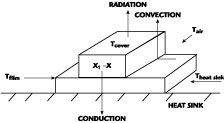
From the experimental data on the heat dissipation for various power levels in an AlN device, a thermal model was used to analyze the temperature variation within the device. The three fundamental modes of heat transfer shown in Figure 13 are used in the analysis.
Radiation
q = ser (T4 s -T4 a )
where
q = power radiated in W/m2
er = emissivity of the solid (0 < er < 1)
s = universal constant called Stefan's constant (5.670 x 10⁻⁸ ) W/m2 K4
Ts = temperature of solid K
Ta = temperature of air in the vicinity of the chip
Convection
q = h(Ts -Ta )
where
q = heat transfer per unit surface W/m2
h = convection coefficient (W/m2 K) it is a function of speed of air on the surface for natural cooling
Conduction

where
q = heat transfer per unit surface W/m2
k = coefficient of thermal conductivity (W/mK)
DX = thickness of the thermal path
When powered up to 75 W, the percentage of heat transfer from the chip determined from the thermal analysis was
Radiation < 0.01 percent
Convection < 0.01 percent
Conduction > 99.98 percent
This analysis applies to an AlN chip at 75 W (normalized) with base temperature maintained at 100°C.
|
|
|
Fig. 14 Temperature profile from thermal analysis data for AlN. |
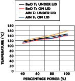
The thermal analysis profile in Figure 14 shows the temperature variation within the chip with maximum temperature of 161°C reached by the resistive element at 75 W, while the base temperature is maintained at 100°C. As a comparison, the temperature reached by the resistive element at 75 W on BeO was only 144°C and that on AlN was 158°C. This shows that BeO is capable of dissipating heat much faster than AlN due to its higher thermal conductivity. A similar comparison can be made for chips with lids attached and at low power, as shown in Figures 15 and 16 , respectively.
|
|
|
|
Fig. 15 Temperature vs. percentage power dissipation profile from thermal analysis. |
Fig. 16 Temperature vs. percentage power dissipation profile from experimental data. |
Conclusion
An extensive and comparative study has been completed both on BeO and AlN as an alternative to BeO for high power resistor and termination applications. Experimental data on BeO and AlN collected and analyzed from production products manufactured in-house revealed that, despite considerable difference in electrical, mechanical and thermal properties, AlN-based high power resistive components can successfully compete with BeO components side-by-side with the added advantage that AlN is non-toxic.
Michael Kettner began working as an RF/microwave technician for Solitron/Microwave in Pt. Salerno, FL, in 1979. He remained there until 1983 and then joined Florida RF Labs Inc., where he moved to process engineering in 1990, was promoted to chief process engineer in 1997 and is currently vice president of operations.
Patrick Biebersmith graduated from South Dakota State University in the spring of 1995 with a BS in electrical engineering. He is currently pursuing a master's degree in electrical engineering. His first position was with Itron Inc. as an RF test and process engineer. Currently he is film products manager and applications engineer for Florida RF Labs Inc.
Nelson Roldan began his career as a system engineer in Guaynabo, Puerto Rico, in 1999. He came to Florida in 2000 where he works as an RF design engineer at Florida RF Labs Inc. He received his degree in electrical engineering from the University of Puerto Rico, Mayaguez Campus (RUM), where he is currently finishing his MSEE degree.
Balram K. Sharma , BSc, MSc, MinstP and CPhys (UK), currently works as a senior process engineer at Florida RF Labs Inc. He has 17 years of work experience in design and process engineering in thick film and thin film technologies including quality assurance engineering. In his previous job he was employed as thin film development manager, passive microwave components, by Midwest Microwave Intl. Ltd., UK.


