Product Feature
An Impedance- Controlled, High Precision Wafer Probe Tip for Applications Up to 40 GHz
Suss/Rosenberger, Germany
Dresden, Germany
|
|
|
Fig. 1 The probe's contact spring assembly and transition to the coaxial air line. |
High precision is a vital prerequisite for the development and manufacture of high frequency cables and connectors to ensure smooth, seamless and low reflection transitions. To achieve this end it is essential that the wafer probe test equipment employed for high frequency applications in laboratories, production lines, and semiconductor research and development is equally precise, as well as reliable and consistent. However, the development of coaxial and planar RF measurement systems demands a completely different approach to that used for low frequencies. In particular, in order to achieve minimum reflections in an RF cable, a defined wave resistance must be maintained along its entire length.
The IZI-Probe has been designed to satisfy these requirements and its unique design features internal reflections not significantly higher than those of the cable connectors up to 40 GHz. These exceptionally low reflections and insertion losses can be achieved because the RF probe uses only air to insulate the RF conductors. In fact, air isolation of the entire probe means that there is also air isolation around the connector and the spring, and there is no coaxial cable used in the transition.
At the probe's core is an air-dielectric coplanar line as the contacting device, which is formed by conductors with a rectangular section. A controlled impedance is defined by the ratio of width to height of the air gap between the contact springs. Even in the area where the springs are held in a dielectric, the gap can be designed to achieve the same impedance. A schematic view of the contact spring assembly and the transition to the coaxial air line is shown in Figure 1 . The central conductor of the coax line ends directly on the inner strip of the coplanar waveguide, and depending on the frequency range, the probes are available with 2.92, 2.4 or 1.85 mm coaxial connectors.
|
|
|
Fig. 2 Time domain reflections of an (a) IZI-Probe and (b) coaxial cable probe. |
|
|
|
Fig. 3 The air dielectric coplanar probe structure; (top) a single three-probe assembly and (bottom) multiple probes on a dielectric support. |
To illustrate its performance, Figure 2 shows a time domain plot of the reflections in an IZI-Probe. The transition from the connector to the probe is shown between the two markers '1,' followed by the transition into a 50 W calibration load. Furthermore, the reduction of the electrical length due to the probe's air isolation compared to a coaxial cable probe with its high dielectric constant can be observed (markers 1 to 2). This demonstrates that the reflection peaks have been reduced to about half that of a standard probe.
The planar structures are manufactured using the highly precise UV-LIGA (a German process for ultra-violet lithography, electroplating and molding) technology. It is only through utilizing newly developed techniques, which facilitate a highly accurate parallelism of the air gap, that has made the design of this new probe tip possible. Nickel is used for the tips due to its good mechanical properties and wear resistance.
The planar structures are 50 mm thick, with an impedance of 50 W being achieved by a gap of approximately 60 mm between each conductor of the coplanar line. In order to ensure this, the thickness of the springs and the distance between them must be kept within a tolerance of approximately 1 mm (see Figure 3 ). The precision of the UV-LIGA is maintained during assembly because the three planar components are fixed onto a dielectric support before separating them. The front ends form the contact springs, which, due to the air gaps, can move independently of each other.
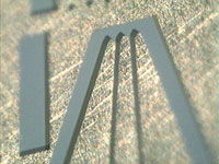
Conventional coaxial probes require vertical and horizontal adjustment, but by utilizing micromachining, this is not an issue for the IZI-Probe. After assembly, the tips are exactly level, so leveling of the tips to the surface of the wafer is not necessary. Precise in-line adjusted contact springs allow reduced over travel and contacting is very reliable due to comparably long, individually flexing tips, which ensure excellent stability of calibration. The probe tips are specified for 1 million touchdowns, although tests have proved the figure to be significantly higher. Figure 4 shows the probe tips in air after 1 million touchdowns on an A1 wafer with A1 dust.
|
|
|
Fig. 4 The IZI-Probe contact tips. |
With coaxial probes a high contact pressure with roughly 70 mm over travel is usual; however, tests on the IZI-Probe have shown that the amount of over travel does not have an effect on the measurement result, which ensures high repeatability. The ISI-Probe works with recommended over travel from only 30 mm. The maximum over travel is 300 mm; however, at that level tip life is shortened. The IZI-Probe exhibits electrical characteristics giving it a high DC capability of over 10W and exact impedance control. Pitches from 50 mm to 500 mm are available.
Conclusion
The IZI-Probe features not only improved electrical performance, but also considerable ease of handling. Leveling is not required and precise in-line adjusted contact springs allow reduced over travel. Furthermore, contacting is very reliable due to comparably long, individually flexing tips, which ensure excellent stability of calibration. It has a very rugged design, which is claimed to be virtually impossible to destroy during normal use. As for the future, a probe designed for operation up to 110 GHz is under development. The IZI-Probe is a collaboration between Karl Suss, Dresden, Germany, and Rosenberger, Tittmoning, Germany.
Karl Suss,
Dresden, Germany,
+49 (0) 352 4073 349.
Circle No.301


