Technical Note
Design and Prototyping of a Transimpedance Front-end Amplifier for Dense Wavelength Division Multiplexing Circuits
As part of the development of an optical power monitor for use in dense wavelength division multiplexing (DWDM) circuits, the effectiveness of a logarithmic operational amplifier transimpedance front-end amplifier was investigated, and the performance of this design compared with a switched gain, linear, transimpedance amplifier (TIA) front-end. The circuit was prototyped using the combination of the MMICAD LAYOUT™ software and the LPKF C60 PCB prototyping machine.
J. Wareberg and D. Kennedy
OPTOTEK LTD.
Kanata, Ontario, Canada
S. Schmidt
LPKF Laser and Electronics
Wilsonville, OR
Time-to-market and design integrity are critical factors in today's fast moving, intensely competitive communication markets. The production of prototype circuits in one's own design facility - using precision milling systems - offers significant advantages of convenience, fast turnaround and protection of intellectual property, without the hazards of harsh chemical processes. Milled circuits more accurately reflect CAD synthesis predictions and indicate the minor corrections that may be needed when replicating prototypes in chemically etched mass production. By taking these variations into account, the designer can be confident that a milled circuit will be as effective as an etched version for the prototyping of new higher frequency devices.
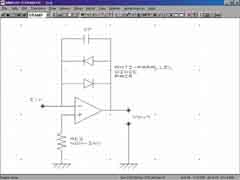
The logarithmic amplifier which was the subject of the prototyping activity is based on the use of an anti-parallel diode pair in the feedback loop of the operational amplifier, as shown in Figure 1 . The current from one of the photodiodes in the photodiode array is fed into the input of the logarithmic amplifier.
|
|
|
Fig. 1 Circuit schematic of a transimpedance amplifier stage. |
The MMICAD LAYOUT™ software was used for circuit layout, and the data exported in the extended Gerber RS-274X format for direct use by the LPKF C60 PCB prototyping machine is shown in Figure 2 .
|
|
|
Fig. 2 LPKF ProMat® circuit board plotter. |
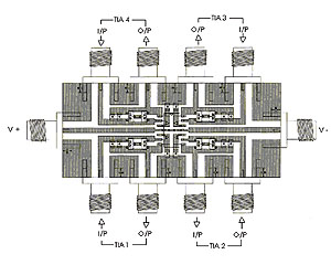
The addition of the extended Gerber RS-274X format is a new feature of MMICAD LAYOUT. (In this extended format, exposure "tool" information is included in a standard way in the data file itself.) Figure 3 shows the MMICAD LAYOUT plot of the layout of a prototype, four channel logarithmic transimpedance (TIA) amplifier stage.
|
|
|
Fig. 3 Transimpedance amplifier layout. |
The prototype was fabricated on 62 mil FR4 material with 1 oz. (35 mm thick) copper clad. The milled amplifier circuit was produced in approximately 15 minutes on an in-house circuit board plotter using built-in software to generate the layout from the downloaded MMICAD design files. The milled circuit provided a very precise mechanical match to the original design pattern in MMICAD because the traces were square and sharp (Figure 4 ), just as they were defined by CAD images and the Gerber 274-X files. The populated PCB, as prepared using the LPKF PCB prototyping machine is shown in Figure 5 .
|
|
|
Fig. 4 Photographs of a 10 mil milling channel machined by LPKF Protomat C60. |
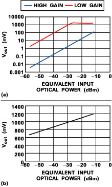
For comparison, Figure 6 shows the wide dynamic range that can be realized using both the switched gain (actually switched feedback resistance) and the logarithmic transimpedance stages.
|
|
|
Fig. 5 The populated printed circuit board. |
The measured RMS noise level as a function of equivalent optical input power is shown in Figure 7 . A photodiode with a responsivity of 0.2 A/W was assumed. To accomplish this, a well quantified current was injected into the front-end of the TIA stage, and the noise level at the output was measured using a precision, low noise, 16-bit A/D converter connected to a computer. In order to minimize the electrical noise contributed by the current source at the input to the TIA, low noise metal film chip resistors were used for the current source.
|
|
|
Fig. 6 Vout vs. equivalent input optical power for the (a) switched gain and (b) diode feedback-based logarithmic transimpedance amplifier. |
From the measured response, it can be seen that the RMS noise level is flat for the linear TIA stage in both the low gain and in the high gain stage. In the low gain state, the RMS noise level is approximately 20 mV, and in the high gain state the RMS noise level is about 100 mV. In practice, the amplifier would be set up to switch from the low gain state to the high gain state when the input optical power level falls below -35 dBm.
The RMS noise level for the logarithmic TIA front-end amplifier increases approximately linearly with decreasing incident optical power level. As the equivalent optical input power decreases, the current from the photodiode into the TIA front-end decreases, causing the small-signal resistance of the feedback diode to increase. As the diode resistance increases, the TIA gain increases, as does the RMS noise level.
|
|
|
Fig. 7 The RMS noise voltage level vs. input power. |
Conclusion
There are merits and disadvantages to the two designs adopted for the transimpedance front-end amplifier. The switched gain circuit is more stable over temperature and time, and the correction procedure is straightforward. The logarithmic transimpedance stage has a larger dynamic range and a uniform dB/mV transfer function, and is a simpler circuit. In terms of noise level, the switched gain circuit has less dependency on optical power level, with different magnitudes for the low and high gain states. The logarithmic circuit exhibits an inverse but approximately linear dependence on optical power. System considerations would dictate the preferred implementation.
In terms of the prototype fabrication activity, the goal of the prototyping work was to arrive at a satisfactory design as quickly as possible while meeting the primary requirement of having the circuit function properly. Superior mechanical accuracy of the prototyping equipment is mandatory. Since most designs are an iterative process, the ability to prepare a finished prototype in minutes allowed the design to progress in an efficient manner. The same design files could have been sent to a local board house for the production of etched prototypes, with typical turnaround of about one week. The wait would necessitate setting the design aside and resurrecting it every time a refinement or revision is made. The accumulated downtime could become a substantial burden for a fast track project.


