
Technical Feature
A Simple VVA RFIC Design with a Focus on Repeatability and Stability
A novel voltage variable attenuator (VVA) integrated circuit reduces the sensitivity of the transfer curves to temperature and process variations. The new solution is achieved without compromising the simplicity of a single positive voltage control design and a large attenuation range. This article describes FET-based VVA characteristics, design trade-offs and common topologies. Following a sensitivity analysis discussion, measured results are presented to show the lower sensitivity of the suggested circuit over a traditional design. Measurements of a large quantity of VVAs, based on the new topology, confirm the robustness of the solution.
Yair Shemesh
Alpha Industries
Woburn, MA
Voltage variable attenuators are important control elements, widely used for automatic gain control both in receive and transmit chains.1,2 When used in handsets, their overall cost and size are of paramount importance. A single positive voltage control scheme and a simple circuit design help in achieving this goal. When operated as part of an open loop gain control, a linear transfer curve simplifies the design of the chain's gain. The unit-to-unit transfer curve repeatability and its stability over temperature are key factors in the ability to design and predict the overall system gain. In receive chains, the VVA is used to control the signal that enters the mixer. It must have a high enough third-order intercept point (IP3) by itself in order not to degrade the overall power linearity. FET VVA topologies such as TEE, PI and bridged TEE are often used,2,3 each with its own merits and problems.
This article reviews the trade-offs among VVA features, and focuses on the issue of stability and repeatability. The reasons for high parameter sensitivities are identified, and based on these identifications, a new VVA topology is suggested. Compared to traditional topologies, the new configuration significantly reduces the sensitivity to process and temperature variations, without sacrificing simplicity, single positive voltage control approach, attenuation range and transfer curve linearity. Several VVAs have been designed and measured based on the new topology. The results clearly show the predicted stability and repeatability improvements.
|
Table 1 | |
|
Emphasis on... |
Causes |
|
High attenuation range |
-Higher sensitivity to process and temperature variations |
|
Transfer curve linearity |
-Increased circuitry complexity |
|
Good repeatability and temperature stability |
-Higher circuit complexity |
|
Lower current consumption |
-Longer settling time |
|
Higher IP3 along the full transfer curve |
-Higher insertion loss |
VVA Design Parameters
The VVA performance is a trade-off among contradicting requirements, as shown in Table 1 . Several FET-based VVA topologies are commonly used. An emphasis on a specific requirement affects the topology selection. For example, the bridged-TEE has superior return losses and a very linear transfer curve, at the cost of complex circuitry and sensitivity to process variations and temperature changes.
|
|
|
Fig. 1 A single positive voltage-controlled TEE VVA. |
The large volume handset production in recent years has emphasized the need for repeatability when selecting a VVA topology. In FET-based VVAs, the device is used as a variable resistor at zero drain source voltage (Vds ). The device parameters vary over temperature, across the wafer and from wafer-to-wafer. Since channel resistance changes sharply for gate-source voltage (Vgs ) close to the pinch-off voltage (Vp ), the stability and repeatability of the transfer curve is governed mostly by Vp . Other FET parameters, such as the ON resistance (Ron ), have a second-order influence on the VVA transfer curve. These parameters are usually correlated to Vp changes in a predicted manner.
In the commonly used topology of a single positive voltage-controlled TEE VVA, shown in Figure 1 , the control voltage Vc is translated into two gate-source voltages.
For the series devices it is given by
Vgsser = Div · Vc - Vcenter (1)
and for the shunt device, by
|
|
|
Fig. 2 Attenuation transfer curve defining top and bottom knees, attenuation range and control range. |

Vgssh = -Div · Vc (2)
where
Div = resistor divider ratio R1/(R1+R2)
Vcenter = fixed DC voltage applied to the series path at the TEE junction
Proper selection of Div and Vcenter for a given Vp allows a roughly linear attenuation dependence on Vc .
At Vc = Vtop knee , the shunt device start conducting (Vgssh = Vp ), while at Vc = Vbottom knee , the series devices start conducting (Vgsser = Vp ). A Vp variation will translate, according to Equations 1 and 2, into a shift of the top and bottom knees. A Vp change by an amount of DVp , shifts the nominal point N by a voltage DVc , to the point R, where
 (3)
(3)
The result, as seen in the ideal curve shown in Figure 2 , is that at Vc = Vtop knee, the attenuation will drop by an amount D[dB] where
D = S · DVc (4)
|
|
|
Fig. 3 An (a) ideal TEE attenuator and (b) implementation with FETdevices. |

S is the transfer curve slope given by DA/DVeff . Therefore, minimizing the attenuation variation D is possible by designing a VVA with small attenuation range DA and a wide control voltage range DVeff . A 12 dB range VVA for a 5 V control voltage was demonstrated by Boglione and Pavio.4
Unfortunately, an attenuation range of more than 30 dB is a more common requirement. Cascading several low attenuation range VVAs is possible for an overall wide attenuation range; however, the overall transfer curve sensitivity will increase as well.
Applying two separate positive controls for the series and shunt devices, and setting Vcenter with a pinch-off follower, can reduce the sensitivity to Vp variations. This can be done at the cost of additional circuitry, based on an operational amplifier, which generates the proper two control voltages.4 In many applications, the need for a simple, low cost, low size VVA solution rules out this option.
A TEE VVA Sensitivity Analysis
In an ideal TEE attenuator, as shown in Figure 3 , the resistors Rsh and Rser should satisfy the matching and attenuation conditions given in Equations 5 and 6, respectively.


|
|
|
Fig. 4 TEE attenuator resistors values for an attenuation range of 40dB, with rser =110W. |

where
A = attenuation in dB
Since for Vgs < Vp , the FET resistance is much higher than 50 W, the series devices should be shunted by a resistor (rser ) that limits the overall series arm resistance to 50 W. For a maximum attenuation of 30 to 40 dB, rser is of the order of 60 to 110 W, depending on the device's periphery and characteristics.
Figure 4 shows the required Rser and Rsh for an attenuation range of 0 to 40 dB, together with the series FET resistance, rnet , for the case of rser = 110 W in shunt with the device.
|
|
|
Fig. 5 Deviation from nominal attenuation due to a 10% Rsh change (a) and 10% Rser change with rser =100W (b) and rser =60W (c). |

Figure 5 shows the deviation from the nominal attenuation of the transfer curve, caused by a change of 10 percent in the shunt device (curve a) and 10 percent in the series device, with the resistor in shunt rser = 100 W (curve b) and rser = 60 W (curve c).
The transfer curve shape is more sensitive to the shunt device resistance variation than to the series device variation, as the shunting resistor rser decreases.
Though the deviation in dB from the nominal transfer curve is smaller for higher Vc (lower attenuation levels), the relative deviation dA/A is larger at low attenuation levels, with a maximum at A = 0.
The New Circuit
One possible approach4 for minimizing the variations is to apply a Vp follower voltage (-Vp ) to Vcenter .
In this case, the Rser deviation from the nominal Rser due to the Vp changes is ideally eliminated since
Rser = f(Vgsser - Vp ) = f(Div · Vc ) (7)
|
|
|
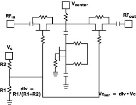
Fig. 6 The new VVA topology. |

Hence, stabilization is achieved for the bottom knee position. The disadvantage of this approach is that the top knee, affected mostly by Rsh , is very sensitive to Vp variations, especially for wide attenuation range, steep slope VVAs. In the newly proposed circuit, shown in Figure 6 , a Vp follower applies a -Vp voltage to the drain and source of the shunt device. The sensitivity of the shunt arm is eliminated since
Rsh = f(Vgssh - Vp ) = f{[Div · Vc - (-Vp )] - Vp } = f(Div · Vc ) (8)
Hence, stabilization is achieved for the top knee position. As previously explained, the series device resistivity mainly affects the bottom knee, which is less critical to the transfer curve shape. Selection of shunting rser resistors low and close to 50 W reduces attenuator sensitivity at the high attenuation levels. Such selection requires high OFF impedance, that is, small gate periphery. On the other hand, a small gate periphery for the series devices increases the loss at the minimum attenuation state. This shunting rser resistor is finally set as a compromise between these two requirements.
|
|
|
Fig. 7 Measured transfer curves of design A (old topology) and design B (new topology). |

The conflict of these requirements is easy to resolve for low attenuation range VVAs and for devices with low normalized drain-to-source capacitance (Cds ).
Results
Several VVAs have been designed, fabricated and measured based on both old and new topologies. Measured transfer curves of the two types of 900 MHz VVAs built to similar specifications are shown in Figure 7 .
While the old topology (design A) has a maximum attenuation at low control voltage, the new one (design B) has maximum attenuation at high control voltage (inverted slope). Other measured parameters are similar for both designs.
Vp variations are caused by process variations and temperature changes.Vp is also the major cause for transfer curve changes. Therefore, transfer curve stability over temperature is an indicator for process variations.
|
|
|
Fig. 8 Change in VVA attenuation when the temperature is increased from 20° to 85° C. |

Figure 8 shows the measured change in the transfer curve when the temperature is raised from +20 to +85°C for the two designs.
It is clearly seen that the new design B deviation is smaller by a factor of 4, compared to design A. Furthermore, since design A maximum deviation is at the low attenuation point of Vc = 3.5 V, the relative deviation dA/A is even worse compared to the dA/A of design B.
VVAs based on the new topology with 3 V control and steeper slope have also been designed and built in large quantities. Measurements confirm the robustness of the solution.
Conclusion
A new VVA topology has been suggested, offering an improvement in stability and repeatability over temperature and process variations.
Acknowledgment
The author wishes to acknowledge the support of D. Johnson and the lab assistance of J. Bedrosian.
References
1. R. Goyal, Monolithic Microwave Integrated Circuits Technology and Design , Artech House Inc., 1989.
2. I. Bahl and P. Bhartia, Microwave Solid State Circuits Design , John Wiley & Sons, New York, 1988.
3. B. Maoz, "A Novel, Linear Voltage Variable MMIC Attenuator," IEEE Transactions on Microwave Theory and Techniques , Vol. 38, No. 11, November 1990, pp. 1675-1683.
4. L. Boglione and R. Pavio, "Temperature and Process Insensitive Circuit Design of Voltage Variable Attenuator IC for Cellular Band Applications," IEEE Microwave and Guided Wave Letters , Vol. 10, No. 7, July 2000, pp. 279-281.
Yair Shemesh received his BScEE and MScEE degrees from the Technion, Haifa, Israel, and has worked for Rafael in Israel and Alpha Industries in the US. His specialties are MW devices, modeling, PAs, RF to MMW MMICs, modules and RF front-ends. He is currently a senior principal engineer at Alpha and can be reached via e-mail at yshemesh@alphaind.com.