TECHNICAL FEATURE
A Method of Measuring Large-signal S-parameters of High Power Transistors
A measurement method for scattering parameters (S-parameters) of high power transistors is presented. The proposed method directly determines the S-parameters of high power transistors by measuring overall gain, phase and S-parameters of input and output matching network when the transistor is operating normally. Using this method, the S-parameters of a small-signal amplifier transistor, Motorola MRF581, and a commercial high power transistor, Motorola MRF6402, are obtained.
Seok Kyun Park, Ik Soo Chang,
Yun Seo Choi, Jun Won Huh
and Young Kim
Sogang University
Seoul, South Korea
To get the optimum performance of a high power transistor, it is essential to obtain the characteristic of the device, such as its S-parameters. In the case of designing a small-signal amplifier, S-parameters are useful and sufficient; however, for a large-signal amplifier, they are no longer useful. This is because the method of measuring the S-parameters of a high power transistor presents a problem.1 Generally, S11 and S21 are measured by the reflection coefficient at the input port and the transmission coefficient at the output port when the input signal is injected at the input port. They are correct values because the transistor is operating normally. S22 and S12 are measured by the reflection coefficient at the output port and the transmission coefficient at the input port when the input signal is injected at the output port. In this case, they are incorrect values because the transistor is not operating normally.2,3
The measurement method of S-parameters of a high power transistor under normal conditions is based on the port reduction technique. This method determines the S-parameters of high power transistors by measuring the overall gain and phase of the measurement system and the S-parameters of the input and output matching networks four times, while the transistor is operating normally unlike the existing method which measures S12 and S22 when the transistor is operating abnormally.
THE THEORY OF THE S-PARAMETERS MEASUREMENT METHOD
The principle of measuring S-parameters under normal conditions using the port reduction technique can be derived as follows. Consider the block diagram of Figure 1.
|
|
[ST ] is the S-parameter matrix of the device under test (DUT), and [Si ] and [So ] are the S-parameter matrices of the input and output matching network, respectively. The S-parameter matrix of the four-port network (dashed line) is given by

If this 4 x 4 matrix is partitioned into 2 x 2 matrices then
B1 = S11 A1 + S12 A2
B2 = S21 A1 + S22 A2 (2)
where

The S-parameter matrix of the transistor is represented by

That is
A2 = ST B2 (5)
Using Equations 5 and 2, B2 is given by
B2 = ST 1 A2 = S21 A1 + S22 A2 (6)
From which A2 can be obtained as
A2 = (ST 1 S22 )1 S21 A1 (7)
Substituting Equation 7 in Equation 2 gives
B1 = S11 A1 + S12 (ST 1 S22 )1 S21 A1 (8)
Therefore, the overall S-parameter between port 1 and port 2, Sall is given by
Sall = B1 A1 1 = S11 + S12 (ST 1 S11 )1 S21 (9)
The matrix of Sall can be written as

and

where
 = S11t S22t S12t S21t
and from Equations 11 and 3

where

Combining Equations 12 and 3 gives

And from Equation 9

Equating S21 in Equation 14 gives

which can be rewritten as
S21all = S21all S22i S11t
+ S21i S21o S21t + S21all S11o S21t S21all S22i S11o  (16)
(16)
where
 = S11t S22t S12t S21t
Therefore, if four different values of the overall S21all are known as well as the S-parameters of the matching networks for the same S21all , a new matrix can be constructed whose elements are S11t , S21t , S22t and  as shown in Equation 17.

and from Equation 17

Equation 18 can be solved without difficulty using the S-parameters of the matching networks (S21i , S22i , S11o , S21o ) and the overall network including the matching networks (S21all ). finally, the S-parameters of the DUT, that is, S11t , S21t , S12t and S22t , can be obtained.
MEASUREMENT METHOD
Figure 2 shows a block diagram of the measurement system used for a large-signal device (MRF6402).
|
|
A preamplifier stage is needed to drive the main amplifier. The output power of the driving amplifier was 27 dBm. However, the output power of the DUT is too high to measure the S-parameters directly with a network analyzer; therefore, a directional coupler (30 dB) is used at output port. In the case of a small-signal amplifier (MRF581), the S-parameters can be measured directly with the network analyzer.
A circulator was used to prevent the driving amplifier from being affected by the reflected signal from the DUT while being tuned.
The tuner was composed of a 3 dB directional coupler and variable sliding shorts. It is possible to realize every point on the Smith chart with this tuner.
The measurement proceeds as follows. The S21all of the overall network that includes only the input and output matching networks can be obtained by compensating the S-parameters of the drive amplifier and output coupler. Then the S-parameters S21i , S22i , S11o and S21o of the matching networks must be measured. This procedure is repeated four times for four different S21all . With this data, the required S-parameters of DUT can be obtained by solving the matrix Equation 18.
EXPERIMENTAL RESULTS
In order to illustrate the capability of this method, experimental results are presented which are obtained from the 1.0 GHz-centered small-signal amplifier (MRF581) biased in class A and the 1.855 GHz-centered large-signal amplifier (MRF6402) biased in class AB (MRF6402, typical output power = 4.5 W, VCE = 26 V, VBE = 0.78 V, ICQ = 40 mA).
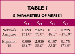
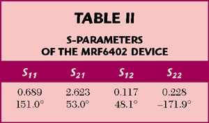
Table 1 shows the S-parameters of MRF581 obtained from solving Equation 18 and measured with a network analyzer. Table 2 shows the S-parameters of the MRF 6402 device obtained by solving Equation 18.
 |
|
To verify the validity of the S-parameters, the gain characteristic of the amplifier is obtained by matching the device using tuners and compared with that of the amplifier matched using the S-parameters from Table 2.
Figure 3 shows the gain characteristic of the amplifier matched with tuners. Figure 4 shows the gain characteristics of the amplifier matched using the measured S-parameters.
 |
|
As can be seen, there was only 0.8 dB difference between the two data. When designing the amplifier, the design technique used the constant gain circle of the small-signal amplifier. As the constant gain contour of the high power transistor is not a circle, the difference between the two approaches is an allowable error.4
CONCLUSION
A novel method for the measurement of the scattering parameters of large-signal transistors has been proposed. Usually, S12 and S22 parameters are respectively obtained with a network analyzer by measuring the reflection coefficient at the collector port and the transmission coefficient at the base port when the input signal is injected into the collector port. This method does not satisfy the transistor's normal operating condition. Therefore, S12 and S22 are not the correct values. However, the method proposed in this article uses only the measured data while the transistor is operating normally. Using this method, the S-parameters of a MRF581 and MRF6402 are obtained, and the validity of this method is verified in each case by comparing the S-parameters measured with the network analyzer with those obtained from the proposed method, and by comparing the gain characteristics of amplifiers using tuners and using the obtained S-parameters. *
References
1. Guillermo Gonzalez, Microwave Transistor Amplifiers Analysis and Design, Prentice Hall, New Jersey, 1997, pp. 212283.
2. S.R. Mazumder, "Two-signal Method of Measuring the Large-signal S-parameters of Transistors," IEEE Transactions on Microwave Theory and Techniques, Vol. 26, June 1978, pp. 417420.
3. Van Valkenburg, Reference Data for Engineers: Radio, Electronics, Computer & Communications, SAMS Publishing, Eighth Edition, 1995, pp. 1217.
4. Guillermo Gonzalez, Microwave Transistor Amplifiers Analysis and Design, Prentice Hall, New Jersey, 1997, pp. 352356.
|
|


 Seok Kyun Park received his BSEE and MSEE degrees from Sogang University, Seoul, South Korea, in 1998 and 2000, respectively. He has worked for Samsung Electronics Co. Ltd. since 2000. His areas of interest are microwave integrated circuits, microwave communication systems and mobile phones. He can be reached at
  Ik Soo Chang received his PhD degree from Seoul National University, Seoul, South Korea, in 1982. He is now a professor at Sogang University. He has more than 20 years of experience in RF and microwave circuits design. He is a member of IEEE. He can be reached at
  Yun Seo Choi received his BSEE from Sogang University, Seoul, South Korea, and is currently working toward his master's degree. His research includes PA design and linearizer system design. He can be reached at
  Jun Won Huh received his MSEE degree from Sogang University, Seoul, South Korea, in 1996. From 1996 to 1999, he was a PA design engineer at KMW, South Korea. He is now a PhD student at Sogang University. His research interests include PA design and linearizer system design. He can be reached at
  Young Kim received his MSEE from Sogang University, Seoul, South Korea, and is currently working toward his PhD degree. He developed Cellular and PCS linear power amplifiers at Samsung Electronics Co. Ltd. His areas of interest are the design of high power amplifiers and linearization techniques, and RF and microwave circuit analysis and design. He can be reached at