
An accurate and flexible large-signal model based on an analysis of the characteristics of InP heterojunction bipolar transistors (HBT) is implemented as a seven-port symbolically defined device (SDD) in Keysight ADS. The model is based on an improved Keysight HBT model formulation, avoiding an erroneous RCICBC transit time contribution from the intrinsic collector region. The model has been verified by comparing simulated and measured DC and small-signal S-parameters at multiple bias points for a 1 x 15 μm2 emitter InP HBT.
InP HBTs in transferred substrate technology have demonstrated excellent high frequency operation, simultaneous with high output power densities.1-2 Compared with a conventional triple-mesa HBT, the transferred substrate technology allows a reduction of the extrinsic parasitic capacitance between the base and collector semiconductor regions of the device. This leads to HBT devices demonstrating extremely high frequency operation, with the potential for active electronics in the sub-THz frequency range, i.e., 0.1 to 1 THz.
There are several available HBT device models (e.g., FBH, University of California San Diego and Keysight) developed specifically for III-V devices.3-4 The UCSD HBT model implements a physical-based charge-control relation, taking heterojunction effects into account. By using an intrinsic collector resistance (RCI), the UCSD model provides reasonable accuracy for the modeling of the knee region; however, a serious shortcoming of the UCSD model, as well as the Keysight HBT model, is that the intrinsic collector resistance is bias independent. Most modern submicron InP HBTs are designed to reach full depletion of the collector at fairly low collector voltages. In this case, the intrinsic collector resistance should be reduced to zero in the model to avoid an erroneous RCICBC transit time contribution, where CBC is the intrinsic base-collector capacitance. This can lead to a significant error in the modeling of the transit time of modern submicron InP double HBT (DHBT) devices with cut-off frequencies in the range of several hundreds of GHz.5
In this work, the unit finger HBT is modeled with an improved HBT model, which corrects the problem of an erroneous transit time contribution from the intrinsic collector region, keeping the ability to model the knee region. Due to improving technology, some new effects occurring in the device can be conveniently added into the SDD in a Keysight ADS simulator. The validity and the accuracy of the large-signal model are assessed by comparing the simulation with the measurement of DC characteristics, small-signal behavior and large-signal operation for a 1 x 15 μm2 InP DHBT.
MODEL DESCRIPTION

Figure 1 Large-signal model without the parasitic elements.
Figure 1 shows the HBT large-signal model, which is based on the Keysight large-signal HBT model. Extrinsic capacitances and inductances are not shown in the figure, as they were removed using electromagnetic de-embedding techniques. ICE is the collector-emitter current, and IBE is the direct base current, representing all recombination processes taking place in the base-emitter junction with forward bias. IBC is the base current in reverse bias, representing hole current injected from the base to the collector, sometimes increased by recombination current in the depletion region. Self-heating is calculated using a simple one-pole RC network, which is commonly used in nonlinear models such as the Keysight, vertical bipolar inter-company (VBIC) and high current (HICUM) models.
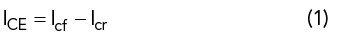
The standard collector-emitter current ICE is composed of the forward and reverse currents Icf and Icr:

IS is the forward collector saturation current, ISR the reverse collector saturation current, VBEi the inner junction voltage of the base-emitter, VBCi the inner junction voltage of the base-collector and NF the forward collector current ideality factor. k is Boltzmann’s constant, q the magnitude of the electronic charge and T the ambient temperature in Kelvin. The formulation for the modification factor DD is based on the UCSD HBT model; its detailed formulas model the behaviors of the Early effect, the heterojunction effects on the collector current for the base-emitter and base-collector junctions and the high current β roll-off effect of a common-emitter I-V plot.
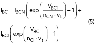
The base-emitter current and the base-collector current cover the ideal and nonideal (i.e., recombination) behaviors.
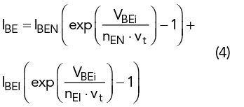
This includes both an ideal component, which is modeled with a saturation current IBEI and ideality factor nEI, comprising the emitter contact and quasi-neutral region recombination and a nonideal component for the space charge region, which is modeled with a saturation current IBEN and ideality factor nEN. The base-collector component is similarly modeled as
To accurately model the DC characteristics, one of the most important physical effects of InP HBTs is the soft knee. The physical reason for this phenomenon is the corresponding injected electron density increases for high level injection, compensating for the collector doping concentration. When the electric field at the base-collector junction is sufficiently reduced, electron transport ceases to be primarily drift current. The rising of the energy band at high current densities blocks electron transport by band energy discontinuity. The effect is equivalent to an increase in the collector resistance, and the voltage drop in the collector resistance causes a reduction of the electric field at the base-collector junction. This resistor is modeled by a bias-dependent collector resistor RCI in this work.5