This article describes an approach to extend the bandwidth of power amplifiers (PA) designed using resistive-reactive series of continuous class F modes (SCFM). By introducing third harmonic loads to the resistive-reactive SCFM PA, the overlap between the fundamental and harmonic impedances is solved and the operating bandwidth extended. Using this approach, a 0.5 to 2.3 GHz high efficiency PA was designed, with experimental results achieving 10 W output power and 59 to 79 percent drain efficiency from 0.5 to 2.3 GHz.
With the rapid development of wireless communications technology, next-generation wireless systems need wider bandwidth to achieve higher data rate transmission. As a key transmitter element, PAs are required to work more efficiently, over broader bandwidths and handle multiple standards.
In recent years, much research has explored improving the bandwidth and efficiency of PAs. In 2009, S. C. Cripps proposed the continuous mode PA to solve the bandwidth limitation of traditional switch-mode PAs, by properly introducing reactive second and third harmonic impedances.1 Continuous class B/J, continuous class F and class F‐1 modes were subsequently proposed.2-6 In theory, the maximum bandwidth of continuous class B/J, continuous class F and class F‐1 PA modes is restricted to an octave due to harmonic impedances at the edge of the Smith chart. Thus, the rigorous requirements of harmonic loads created difficulty realizing multi-octave performance. The resistive-reactive series of continuous modes was proposed by Lu and Chen in 20137 to relax the strict demands of harmonic loads, introducing resistive harmonic impedances to the continuous modes.8-9 With this approach, the bandwidth can exceed an octave by introducing resistive second harmonic loads and a more extensive fundamental impedance space, extending the bandwidth of broadband PAs. The resistive-reactive series of inverse continuous modes PA proposed by Li et al.9 illustrates similar properties for the design of broadband PAs.
In this article, an extended mathematical formula is applied to the resistive-reactive SCFM. The design space is further extended by introducing third harmonic impedances, providing more freedom when designing high efficiency multi-octave PAs.
Extended Resistive-Reactive SCFM
The traditional resistive-reactive SCFM has a half-wave rectified sinusoidal current waveform, ids(θ), at the intrinsic current generator plane of the device:

The voltage waveform, vds (θ), is no longer rigorously restricted to a square waveform and includes a set of variations dependent on the parameters α and γ:

Resistive third harmonic impedances are introduced by multiplying the current waveform of the resistive-reactive SCFM by the factor (1+β cos θ), while the voltage waveform remains unchanged. The new current waveform is represented by:

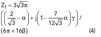
Alternative impedance solutions with resistive second and third harmonic impedances can be obtained. The load impedance to be presented at each harmonic is calculated by dividing the voltage by the current. Here, Zn is designated as the nth-order harmonic impedance. Thus, the normalized harmonic impedances can be calculated from:


The feasibility of Z1, Z2 and Z3 depends on the conditions
0 ≤ α ≤ 1 and −8/3π ≤ β ≤ 0
being fulfilled. Figure 1 illustrates the variation of the fundamental and harmonic impedances vs. α and β. The second harmonic region moves toward the fundamental region with variation of α and β, and the third harmonic region approaches the fundamental region with decreasing β. This characteristic makes solving the overlap between the fundamental and harmonic impedances in a multi-octave design possible.

Figure 1 Fundamental and harmonic impedances vs. α and β.
Drain efficiency can be calculated from Equations 2 and 3 as:

Drain efficiency is a function of α and β. The variation of drain efficiency and output power with respect to α and β are shown in Figure 2. The variation of α and β should be restricted within a limited region to achieve acceptable drain efficiency with a slight degradation of output power. In this work, the conditions of 0 ≤ α ≤ 0.4 and −0.4 ≤ β ≤ 0 are selected to achieve drain efficiency greater than 65 percent.

Figure 2 Drain efficiency (a) and normalized output power (b) vs. α and β.
Simulation and Measurement
To verify the effectiveness of this approach, a 0.5 to 2.3 GHz resistive-reactive SCFM PA was designed using a Wolfspeed CGH40010F GaN transistor, operating at a quiescent drain bias of 28 V and of 68 mA, and a 30 mil thick Rogers 4350B substrate (εr = 3.66) with a conductor thickness of 35 μm.
The optimum load impedances were obtained by harmonic load-pull simulation using an iterative process from high to low frequency, where the impedance obtained at the high frequency was used to terminate the low frequency harmonic. This was repeated until the optimum load impedances were obtained. The output matching network was designed using the real frequency direct computational technique.10 Figure 3 shows the broadband output matching network for this design. Due to the small effect of input harmonic impedance on performance,11 when designing the input matching network, more attention was paid to fundamental matching.
