
Reduced Filter Requirements Using an Ultra Low Noise Modulator
RF Micro Devices
Greensboro, NC
Each new generation of the mobile phone is specified to support multiple standards and provide new and more complex applications, such as higher data rate capability. At the same time, it is expected that improvements be made to talk time, standby time, and to reduce size, weight and cost. These technical goals, demanding greater and greater innovation, present a significant challenge to the mobile phone design team. Innovation sometimes means inventing something new; in other cases it means improving on familiar circuits or architectures. In the case of direct quadrature modulation, innovation is being applied to performance improvements allowing a well-known architecture to be used in handsets and base station applications, while helping to meet those challenging goals.
In this article, historical transmit approaches used in mobile phones are presented with specific attention to direct quadrature modulators. The inherent benefits of direct modulation are described, including reduced system complexity and filtering requirements specifically when compared to upconversion-based systems.
With the introduction of Enhanced Data rates for GSM Evolution (EDGE), the use of a direct quadrature modulator is being re-evaluated for mobile phone applications. A discussion is presented showing where the use of a direct quadrature modulator is especially attractive when used with a GSM transceiver. This approach preserves the talk time associated with GSM handsets, while adding the EDGE capability for data applications. It is shown that if certain essential broadband noise performance goals are met, the use of direct quadrature modulation can have a significant impact on reducing size, weight and power consumption of mobile phones.
TRANSMIT ARCHITECTURES
Transmitters perform modulation, upconversion and power amplification. When modulation and upconversion are performed in two steps, the architecture is called dual conversion or two-step conversion, as shown in Figure 1. When modulation and upconversion are performed in one step, the architecture is called direct conversion.

A third type of transmit design is called translational loop or offset phase-locked loop (OPLL). These approaches use a phase-locked loop at the RF output to minimize external filtering by acting like a tracking narrowband, bandpass filter. This system was defined before 19801 , and was later commercialized for GSM handsets to reduce cost and power consumption.3
DUAL CONVERSION TRANSMITTERS
In dual conversion transmitters, the modulator performs the modulation and a portion of the upconversion, and a second block, an upconverting mixer, performs the rest of the upconversion to RF. It is also possible to use more than two steps to upconvert the baseband signal to RF.
The primary benefit of a two-step transmitter is that narrowband filtering and gain control can be implemented efficiently at the IF. The architecture also benefits from the local oscillator operating at a different frequency from the RF. This avoids an issue called injection pulling,2 seen when using direct conversion in the receive or transmit paths.
Many of today's CDMA and TDMA mobile phones include the two-step transmitter approach. When compared to direct conversion, this approach has proven to be less problematic but requires the addition of filters at both the RF and IF. The IF filter is required to attenuate the wideband noise floor and the higher harmonics of the IF generated by the in-phase and quadrature (I/Q) modulator. The RF filter is required to attenuate the unwanted sidebands and spurs generated from the upconverting mixing process.
Another issue when using a two-step transmitter is providing the LO frequencies for both the first and second upconversion steps. When compared to direct conversion/modulation, the two LO signals must be generated, which may require a second phase-locked loop (PLL).
TRANSLATIONAL LOOP ARCHITECTURE
The benefit of a translational loop approach is it achieves a low noise floor allowing the duplexer to be replaced with a switch. The elimination of the duplex filter, with its associated insertion loss, allows the power amplifier to operate at a lower output power.
Two variants of this approach are described. Figure 2 shows a transmit line-up that consists of a quadrature modulator, an offset downconverting mixer, a phase comparator, loop filter and VCO.3 The TX LO frequency is offset from the TX carrier frequency by fIF (fVCO = fLO fIF ). The offset PLL acts as a tracking bandpass filter tuned to the desired channel frequency. This approach reduces the wideband noise floor providing a benefit over the standard upconversion approach, where the sideband noise would require an additional filter and typically a duplexer.

Figure 3 shows a variant of the translational loop that includes the quadrature modulator within the feedback loop.4 This approach includes an I/Q modulator, a downconverting mixer, a phase detector with charge pump outputs, two programmable counters, a loop filter and VCO. A benefit of this architecture is that the programmable dividers provide additional flexibility in frequency planning.

In GSM, where the modulation is a constant envelope signal, all of these architectures can use a class-C power amplifier providing good power-added efficiency (PAE). An added benefit of the translational loop systems is the VCO strips off any residual AM component allowing a class-C amplifier to be driven even harder, providing additional PAE.
DIRECT QUADRATURE MODULATION
Direct quadrature modulation, as shown in Figure 4, is a common form of direct conversion used in the transmit path. This architecture offers several advantages over the two-step or translational loop transmitters since neither a second LO or an intermediate PLL is required. In addition, an upconverter is not needed since the modulator performs the upconversion to RF. When compared to the translational loop, no feedback loop is required, which includes an additional mixer, phase detector, dividers and loop filter.

Historically, direct quadrature modulators have been used in several handsets, but usually require a duplex filter to meet specifications for noise in the receive bands. The translational loop has largely replaced other architectures for constant envelope modulation formats since its low output noise and spurs eliminate the duplex filter.
MINIMIZING TRANSMIT PATH RF FILTERING
The RF2483 ultra low noise direct quadrature modulator has been developed to offer a possible migration path for existing GSM mobile phones to support linear modulation schemes, such as EDGE in the transmit path. The receiver architectures of existing GSM mobile phones are typically capable of supporting most modulation formats. The migration to EDGE, with its 3π/8 8PSK modulation format, should not require a major re-architecture of the receive path, although the specifications of the individual blocks may require tightening.
In the transmit path, the situation is not so straightforward. Over the past ten years, the GSM handset's major gains in talk time have been achieved through the elimination of costly duplex filters. This has been enabled by the adoption of translational loop architectures and, more recently, fractional N synthesizers6 for signal modulation. These two transmit techniques rely on the constant envelope properties of the GSM modulation and are not directly applicable to EDGE with its linear 3¼/8 8PSK modulation format.
The ultra low noise RF2483 direct quadrature modulator, shown in Figure 5, is well suited for use in a linear transmit path. This modulator allows for the elimination of filters, which results in lower power consumption and savings in both cost and board area. The elimination of RF and IF filtering enables the transmit path to simultaneously cover both the PCS1900 and DCS1800 frequency bands, as well as supporting GSM, EDGE and TDMA in the same mobile phone.

QUADRATURE MODULATOR APPLICATIONS
The previously shown example of a generic direct quadrature modulation transmit architecture can be used for any type of modulation. This simple architecture can benefit from a relaxed RF filtering requirement, the need for a single synthesizer and fewer spurious problems over a dual conversion transmitter architecture. The key problem when using a direct quadrature modulator is the injection pulling of the LO due to the presence of an RF carrier at the LO frequency.
Injection pulling of an on-frequency transmit VCO can be caused by the signal power coupling back from the power amplifier (PA) output. This causes corruption of the LO signal's spectral integrity with subsequent degradation in the modulated signal quality.2 Despite this problem, by using direct quadrature modulators with on-frequency VCOs, GSM transmitters have been successfully manufactured in mass production.7,8
To reduce sensitivity to LO pulling, a variety of possible solutions are available. These include LO generation through the use of offset mixing with a second uncorrelated LO signal,9,10 offset mixing with a divided version of an LO signal and the LO itself,11 frequency doubling,12 frequency dividing,13 fractional division/multiplication using a regenerative mixer11 and wide bandwidth on-frequency PLLs.3
The sensitivity of pulling to an on-frequency VCO can be reduced by using a PLL with a loop bandwidth that is much greater than the modulation bandwidth.14 The lower susceptibility to pulling is demonstrated in the existing GSM translational loop architectures, where the power VCO is at the same frequency as the TX signal. The translational loop's PLL, with its high unity gain bandwidth of approximately 1.5 MHz, provides sufficient pulling protection, eliminating the need for special shielding.
With EDGE modulation, the change from a constant envelope modulation format to 8-PSK has implications on VCO pulling which must be investigated further. However, in GSM, large amounts of AM are present during the start of the burst, when the PA output power has to ramp up rapidly. Using a wide loop bandwidth does not solve the pulling problem in linear modulation schemes, although it is a severe test of the loop's susceptibility to pulling.
EXTENDING GSM TX ARCHITECTURE FOR EDGE AND TDMA
A possible migration path is now introduced for existing GSM mobile phones to support linear modulation schemes in the transmit path. The migration is based on an add-on to existing GSM solutions that could be implemented using commercially available GSM transceiver ICs, as shown in Figure 6. The EDGE (and possibly TDMA and W-CDMA) extensions to the transmitter are achieved through a parallel direct quadrature modulation transmit path. It is proposed that LO generation for the transmit path is achieved through reuse of the GSM transmitter's translational loop VCO.

The receive band noise specifications are achieved through use of an ultra low noise dual band modulator with automatic gain control (AGC). The frequency bands for EDGE are the same as those used for GSM. Therefore, frequency planning is automatically obtained through the re-use of the GSM transmitter's translational loop VCO.
The VCO's sensitivity to pulling is reduced by using the translational loops' wide PLL loop bandwidth (~1.5 MHz)3 for LO generation. Good power efficiency is maintained by keeping the loss between the PA and antenna to a minimum, and by being able to operate the PA at relatively high PAE without concern for noise folding.
RECEIVER BAND NOISE
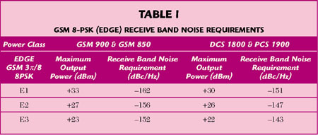
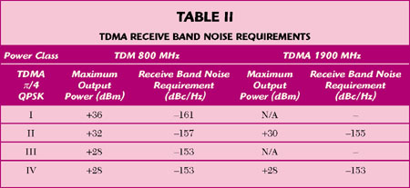
The typical receive band noise requirements for EDGE and TDMA systems are listed in Tables 1 and 2. Cellular band EDGE transmitters require their transmitted RX band noise floor to be less than 152 dBc/Hz, and all TDMA transmitters require receive band noise to be less than 153 dBc/Hz.
Until recently, commercially available direct quadrature modulators have not been capable of meeting the TDMA or EDGE receive band noise requirements without additional RF filtering. The introduction of the RF2483 ultra low noise dual band quadrature modulator with AGC makes it possible to design a linear transmit path without the need for any RF bandpass filters for certain classes of TDMA/EDGE handsets.
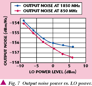
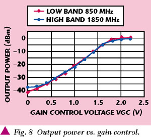
The RF2483 IC meets these requirements with a broadband noise floor of 156 dBc/Hz, measured at 0 dBm output power with an output third-order intercept point (OIP3) of +18 dBm, as shown in Figure 7. The noise floor is approximately 16 dB lower than other commercially available direct quadrature modulators. The device also offers a gain control function which helps the systems designer manage the gain/noise and distortion budget in the transmit path as power control is applied, as shown in Figures 8 and 9.

The design of a low noise transmit path is essential to optimize the power consumption. Filtering after the PA must be avoided due to power consumption penalties associated with the insertion loss of the filter at high power levels. Filtering prior to the PA is ineffective due to a noise folding phenomenon (see the noise folding sidebar). Under certain circumstances, transmit band noise can be translated in frequency into receive band noise with a conversion gain of approximately 10 dB.
If the transmit chain's RX band noise is filtered prior to the PA, and the TX band noise is still greater than 146 dBc/Hz, then noise folding means that filtering typically must occur after the PA. This has obvious implications on power consumption due to the insertion loss of the filter at full power levels. One possible alternative is to perform RF filtering prior to the PA, and operate the PA at lower PAE, where the amplifier is more linear and the noise folding gain is lower. Operating the PA at a lower PAE results in higher power consumption; however, it is still lower when compared to filtering after the PA.
CONCLUSION
It has been shown that the use of a direct quadrature modulator provides significant benefits to the handset designer when trying to meet the challenging goals brought on by the third generation of mobile phones. Direct quadrature modulators provide high performance and reduced system complexity, helping reduce the size and cost of mobile handsets. With the achievement of low broadband noise in the RF2483 modulator IC, transmit filtering is minimized, which lowers power consumption and the overall cost of the handset. Finally, it was demonstrated that by using a direct quadrature modulator with a GSM transceiver, EDGE could be implemented while maintaining GSM talk time. *
References
1. F. Gardner, "Translation Loops," Phaselock Techniques, 1979, pp. 20420.
2. B. Razavi, "RF Microelectronics," pp. 152155.
3. T. Yamawaki, et al., "A 2.7 V GSM RF Transceiver IC," IEEE Journal of Solid-State Circuits, Vol. 32, No. 12, December 1997.
4. G. Irvin, et al., "An Up-conversion Loop Transmitter IC for Digital Mobile Telephones," ISSCC, 1998 Digest of Technical Papers, pp. 364365.
5. RF Micro Devices "RF2483 Dual Band Quadrature Modulator with AGC," data sheet, www.rfmd.com.
6. J. Sevenhans, "Silicon Radio Integration," Architectures and Technology IEEE200 Custom Integrated Circuits Conference.
7. J. Fenk, "Highly Integrated RF ICs for GSM and Dect Systems A Status Review," IEEE Transactions on Microwave Theory and Techniques, Vol. 45, No. 12, December 1997.
8. J. Stevenhans, et al., "An Analog Radio Front-end Chip Set for a 1.9 GHz Mobile Radio Telephone Application," ISSCC, 1994.
9. J. Riska, et al., "Local Oscillator Generation for Direct Conversion Transmitters," Analog Integrated Circuits and Signal Processing, Vol. 22, No. 1, January 2000.
10. T. Stetzler, et al., "A 2.7 V to 4 V GSM Transceiver RF IC," ISSCC, 1995.
11. J. Strange and S. Atkinson, "A Direct Conversion Transceiver For Multi-band GSM Application," 2000 IEEE Radio Frequency Symposium.
12. S. Heinen, et al., "A 3.0 V 2 GHz Transmitter IC for Digital Radio Communication with Integrated VCOs," ISSCC, 1995.
13. M. Moffat, et al., "An ISM Band Transceiver Chip for Digital Spread Spectrum Communication," ESSCIRC, 1997.
14. J. Crols and M. Steyaert, "CMOS Wireless Transceiver Design," p. 66.
APPENDIX A
NOISE FOLDING
If a desired carrier signal and band limited noise is applied to the input of a nonlinear amplifier, as shown in Figure S1, then transmit band noise will be folded around the carrier frequency. The TX band noise may be translated in frequency to become receive band noise. The conversion loss of this noise folding is a complex function of the class of amplifier, carrier and offset frequencies, modulation format, circuit topology and terminating impedance at both in-band and out-of-band frequencies. The noise folding mechanism has similar origins to third-order intermodulation. It correlates reasonably well to intermodulation measurements where the first tone is at the desired carrier signal amplitude and the second tone is at least 30 dB below the first, as shown in Figure S2.


NOISE FOLDING MEASUREMENTS FOR A LINEAR PA
To illustrate the noise folding phenomena, a desired signal with band-limited noise was ap-
plied to a linear PA, as shown in Figure S3. Figure S4 shows the measured results of the noise folding conversion gain and output power verses input power for a typical linear cellular band PA. The two noise folding gain plots at 5 and 20 MHz offsets illustrate the dependence on the frequency offset from the carrier signal.


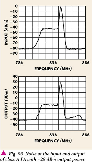
Spectral plots for a PA operating in a saturated mode are shown in Figure S5. The PA is operating in class C mode with a PAE of 50 percent. This amplifier is highly nonlinear, and its noise folding conversion loss can be as low as 3 dB, and may even turn into a conversion gain under certain unfavorable conditions.

Figure S6 shows the same PA operating at 4 dB below its maximum output power. This corresponds to an amplifier in its linear mode where the amplifier is operating class A with a PAE of 30 percent. The amplifier obviously suffers from lower amounts of distortion; however, it is still sufficiently nonlinear for the conversion losses to be between 10 and 15 dB depending on the specific conditions.
RF Micro Devices,
Greensboro, NC (336) 664-1233.
Circle No. 303