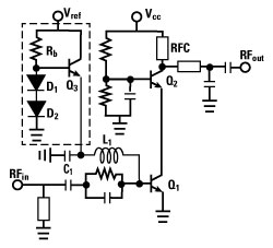
Figure 3 Single stage, cascode U-Band PA.
U-BAND PA DESIGN
The unit emitter area of the high speed HBT is 0.5 × 10 μm2. For a cascade active core, 18 fingers (18 × 0.5 × 10 μm2) are used for both the CE (Q1) and CB (Q2) transistors (see Figure 3). To regulate the DC bias current of Q1 over process, temperature and DC supply variations, Q3, D1 and D2 form a voltage compensation bias network at the base of Q1. The active base bias transistor, Q3, employs eight fingers of a high speed HBT (8 × 0.5 × 10 μm2). Input and output matching circuits are composed of MIM capacitors and on-chip microstrip with top thick metal lines. For compact size, spiral inductors are not used in the matching circuits.
The output power of the n-stacked PA can be expressed as4

where n is 2 for this PA. Ropt_PA, Vce, Vk and Id are the optimum output load impedance, collector-to-emitter voltage, knee voltage and DC supply current, respectively. Ropt_PA is

where RL is the load impedance of each stacked transistor. From Equation 9, Ropt_PA increases with RL. Since the DC currents across each transistor of the stacked PA are all the same, the output power can be enhanced by stacking the transistor.
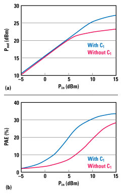
Figure 4 Simulated output power (a) and PAE (b) of a U-Band PA at 52 GHz, showing the effect of C1.
A constant base voltage has been suggested for obtaining both high output power and high efficiency in an HBT PA.8 To achieve this for Q1, the simulated minimum inductance value of L1 is 3 nH; however, a high L1 inductance increases the size of the PA MMIC. Alternatively, a shunt capacitor, C1, is used to reduce the MMIC size by lowering the value of L1. Based on a load-pull simulation, two-section LC elements are designed for the output matching network. A one-section LC element is employed for the input matching network of the stacked PA, and an RC network is added to the base of Q1 for circuit stabilization.
Figure 4 shows the simulated output power (Pout) and PAE of the U-Band PA at 52 GHz with and without capacitor C1. For the simulation, 0.8 nH for L1 and 0.1 pF for C1 are used. Without C1, RF leakage to the bias transistor Q3 would cause a voltage drop through the base and emitter in the negative direction, resulting in a base voltage increase for Q1 with increasing input power. The increased collector current of Q1 would then unnecessarily lower the Pout and PAE of the power amplifier in the high output power region.
MEASURED RESULTS
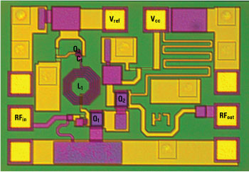
Figure 5 Fabricated U-Band PA MMIC.
The fabricated U-Band PA MMIC (see Figure 5) contains input and output matching circuits, an active bias circuit and probing pads and is laid out in an 0.88 mm × 0.67 mm (0.59 mm2) area. The PA MMIC is biased with Vcc = 5 V and Vref = 2.5 V and draws a quiescent current of 120 mA. Figure 6 shows the measured small-signal performance of the PA from 45 to 60 GHz. The measured linear gain is about 14.2 dB at 52 GHz, with more than 35 dB isolation. At 52 GHz, the measured 1 dB compression output power (P1dB) and saturated output power (Psat) are 21.2 and 25.97 dBm, respectively, as shown in Figure 7a. The measured PAE versus input power is shown in Figure 7b. At 52 GHz, the peak PAE is 28.7 percent. The measured performance of the U-Band PA is in good agreement with the simulation shown in Figure 4.
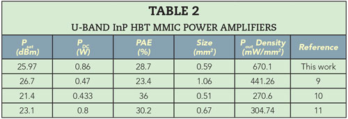
A comparison of U-Band InP HBT PAs is shown in Table 2.9-11 The output power density of 670.1 mW/mm2 is the highest demonstrated for an InP HBT PA.
CONCLUSION
A compact U-Band PA with an on-chip active bias circuit using a commercial 0.5 μm InP HBT process has been demonstrated. The fully matched PA MMIC exhibits an output power density of 670.1 mW/mm2, which, to our knowledge, is the highest value reported for a U-Band InP HBT PA.
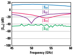
Figure 6 Small-signal performance of the U-Band PA MMIC.
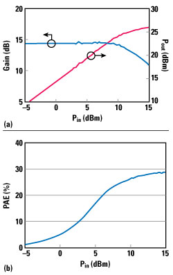
Figure 7 Measured gain and output power (a) and PAE (b) vs. input power.
References
- J. Park, C. Lee and C. A. Park, “A Quad-Band CMOS Linear Power Amplifier for EDGE Applications Using an Anti-Phase Method to Enhance its Linearity,” IEEE Transactions on Circuits and Systems-I: Regular Papers, Vol. 64, No. 4, April 2017, pp. 765–776.
- Z. Zhao, Z. Tang and Y. Wu, “Broadband High Efficiency Power Amplifier Design Using Continuous Class F Mode,” Microwave Journal, Vol. 60, No. 5, May 2017, pp. 132–146.
- Y. Sun, X. Zhu and F. Meng, “Simple Synthesized Harmonic Matching Strategy in Broadband PA Design,” Microwave Journal, Vol. 58, No. 10, October 2015, pp. 88–98.
- C. C. Shen, H. Y. Chang and Y. C. Wang, “A Monolithic 3.5-to-6.5 GHz GaAs HBT-HEMT/Common-Emitter and Common-Gate Stacked Power Amplifier,” IEEE Microwave and Wireless Components Letters, Vol. 22, No. 9, September 2012, pp. 474–476.
- J. L. Zhao, E. Rahimi, F. Svelto F and A. Mazzanti, “A SiGe BiCMOS E-Band Power Amplifier with 22% PAE at 18 dBm OP1dB and 8.5% at 6 dB Back-Off Leveraging Current Clamping in a Common-Base Stage,” IEEE International Solid-State Circuits Conference Digest, February 2017, pp. 42–43.
- J. Ko, D. Kim and S. Jeon, “D-Band Common-Base Amplifiers with Gain Boosting and Interstage Self-Matching in 0.18 μm SiGe HBT Technology,” IEEE Transactions on Circuits and Systems II: Express Briefs, Vol. 63, No. 3, March 2017, pp. 254–258.
- B. W. Min, M. Chang and G. M. Rebeiz, “SiGe T/R Modules for Ka-Band Phased Arrays,” IEEE Compound Semiconductor Integrated Circuit Symposium, November 2007.
- Y. S. Noh and C. S. Park, “PCS/W-CDMA Dual-Band MMIC Power Amplifier with a Newly Proposed Linearizing Bias Circuit,” IEEE Journal of Solid-State Circuits, Vol. 37, No. 9, September 2002, pp. 1096–1099.
- H. C. Park, S. Daneshgar, J. C. Rode, Z. Griffith, M. Urteaga, B. S. Kim and M. Rodwell, “An 81 GHz, 470 mW, 1.1 mm2 InP HBT Power Amplifier with 4:1 Series Power Combining Using Sub-Quarter-Wavelength Baluns,” IEEE MTT-S International Microwave Symposium, June 2014.
- Z. Griffith, M. Urteaga, P. Rowell and R. Pierson, “71–95 GHz (23–40% PAE) and 96–120 GHz (19–22% PAE) High Efficiency 100–130 mW Power Amplifiers in InP HBT,” IEEE MTT-S International Microwave Symposium, May 2016.
- H. C. Park, S. Daneshgar, J. C. Rode, Z. Griffith, M. Urteaga, B. S. Kim and M. Rodwell, “30% PAE W-Band InP Power Amplifiers Using Sub-Quarter-Wavelength Baluns for Series-Connected Power-Combining,” IEEE Compound Semiconductor Integrated Circuit Symposium, October 2013.
