
Design Considerations for Thick-film High Power Chip Terminations
Robert Grossbach
American Technical Ceramics
Huntington Station, NY
As the wireless revolution extends component requirements upward in frequency, higher in operating power and smaller in size, the performance demands on surface-mount devices grow ever more stringent. Chip terminations made with resistive films are typically used to absorb power that appears at the normally isolated ports of couplers or hybrids, power resulting from mismatches, imperfect directivity, or imbalances somewhere in the system. Reliable designs place conservative limits on the maximum temperature of the resistive film and use substrate materials that closely match the film's coefficient of thermal expansion (CTE). This article discusses three strongly interrelated aspects of thick-film termination design: materials and processes, thermal management, and RF impedance matching.
To limit the resistive film's temperature an insulating substrate with high thermal conductivity is required. Other desirable properties include a temperature-independent (over a reasonable range) dielectric constant at microwave frequencies, physical strength, good adhesion to thick film resistive materials, and imperviousness to humidity and processing chemicals used in microelectronic assembly. For many years in the US, beryllium oxide (BeO) has been the substrate of choice to meet these requirements -- despite the fact that BeO dust and powder are known to be hazardous, and require special handling and disposal techniques. However, the international community has opposed the use of BeO, and so in recent years an alternate material, aluminum nitride (AlN) has found increasing use as a substitute. Table 1 compares typical properties of AlN to BeO; data for 99 percent alumina is included for reference.

While there are a number of thick-film resistive materials available, one based on ruthenium oxide (RuO2 ) is currently employed by several leading manufacturers. RuO2 , when combined with several (usually proprietary) additives, yields a film that adheres well to AlN, exhibits excellent parametric stability with time and temperature, and can be conveniently re-fired to adjust its resistivity.
DESIGN EXAMPLES
AlN and an RuO2 based thick film will be utilized to illustrate the considerations involved in the design of three chip terminations with the following specifications: Unit A -- DC to 6000 MHz frequency range; power dissipation = 20 W at an ambient temperature of 50°C; maximum VSWR of 1.15; unit B -- DC to 4000 MHz frequency range; power dissipation = 200 W at an ambient temperature of 50°C; maximum VSWR of 1.15; unit C -- same as unit B, except power dissipation = 600 W.
A thick-film coated ceramic chip is shown in Figure 1 . A metallic wraparound -- nominally a short circuit -- connects one end of the film to the metallized ground covering the chip's bottom surface. Three simplifications will be made in order to establish an elementary thermal model: The heat is generated uniformly everywhere in the film; the heat flow is laminar -- no fringing -- from the film to the bottom of the chip, which is assumed at ambient (thermal ground); there is no convective or radiative heat flow. Concerning uniform heat generation, the currents in the film are edge concentrated, hence there will be more heat generated at the edges than at the center. Nevertheless, the approximation is expected to be reasonable for film geometries where the length and width are substantially greater than the substrate thickness. Additionally, tapers are not being considered, wherein the width of the film and hence the power dissipated at any cross-section may vary along its length. Concerning laminar heat flow, it is understood that there is indeed thermal fringing, not only from the front face of the film -- heat flow lines shown dotted in the diagram -- but from the lateral edges as well. Thus, the second and third assumptions are conservative -- there will be additional heat paths beyond those accounted for -- while the first will need further investigation since edge-located hot spots could develop at RF that would not be revealed in DC tests.

The basic formula for steady state heat flow is given as

where
|
T |
= |
temperature of film (°C) |
|
TA |
= |
ambient temperature (°C) |
|
P |
= |
power dissipated in film (W) |
|
D |
= |
substrate thickness (m) |
|
A |
= |
area of film (m2 ) |
|
k |
= |
thermal conductivity (W/m°C) |
A 40-mil chip thickness is assumed for mechanical strength and substrate availability at moderate price, and the maximum film temperature will be limited to 150°C. Using the thermal conductivity of AlN at 200°C, and setting P = 20 W, it is determined from Equation 1 that to limit T to 150°C (max) (100°C above specified ambient) requires a film area of 2624 mils2 . For P = 200 W, the film area is 26,240 mils2 .
Next, the conditions that insure the film behaves as a constant resistance through the highest operating frequency are examined. As is well known, skin effect causes currents to decrease inside conductors, thereby increasing their effective resistance as the frequency increases. For a flat plane conductor of finite thickness D it may be shown1 that if the conductor thickness is one-half the skin depth, the conductor will have virtually the same resistance as its DC value. Skin depth (d ) is given by

where
|
r |
= |
resistivity of film (W -m) |
|
f |
= |
frequency (Hz) |
|
µ |
= |
permittivity of film (H/m) |
The film thickness Tf is typically fixed at approximately 0.5 mils. If d = 2Tf = 1.0 mils = 2.54 × 10?5 m, Equation 2 can be solved for r at the highest operating frequency, 6 GHz. The result is that values of r = 15.3 x 10?6 W -m yield skin depths = 1 mil. The low frequency resistance (W ) of the film is given by

For a 0.5 mil thick square film, this corresponds to RL = 1.5 W /sq. Since film resistances are readily available in values ranging from 10 to 1000 W /sq, this value is not restrictive.
EQUIVALENT CIRCUIT
Next, an equivalent circuit is derived for an unmatched termination by considering the admittance of a shorted section of lossy line. This admittance is given by

where l is the line length and Y0 , the characteristic admittance, is

and  , the propagation constant, is

R, L, G and C are the resistance, inductance, conductance, and capacitance per unit length, respectively; w is the angular frequency = 2p f. For a low loss substrate such as AlN, G can generally be neglected compared to w C. To obtain a lumped equivalent circuit for the shorted transmission line, a power series expansion for coth x = 1/x + x/3 ? x3 /45 + ... is used, where |x| < p . Then, taking the first two terms of the series, Equation 4a becomes

Yin is recognized as the admittance of the circuit shown in Figure 2 . The inductance and capacitance impose limits on how well matched the termination can be made over a given bandwidth.

For efficient use of the substrate area and to avoid very large discontinuity reactances, it is usually desirable to keep the film length-to-width ratio not far from unity. At this point, some actual equivalent circuit component values may be checked for a square shape. Under Equation 1 it was determined that for thermal reasons the film area for unit A (20 W) must be 2624 mils2 minimum; therefore, line width and length must be 51.2 mils. Using standard microstrip formulas2 for a lossless transmission line of the same dimensions as the lossy line, on 40-mil-thick AlN, this results in a characteristic impedance Z0L of 45.9 W and a group velocity of 4.86 × 10⁹ in/s. Noting that

and

the inductance and capacitance per unit length can be calculated. Per results under Equation 5, and referring to Figure 2, if the film length is l, the total inductance L'l = Ll, and the total capacitance, C'2 = Cl/3. Results for units A and B are listed in Table 2 . Smith Chart reflection plots of units A, B and C, modeled on a CAE program,3 are shown in Figure 3 .

It should be noted that there are several approximations involved in the above derivations and table: The microstrip formulas apply to lines on infinitely wide ground planes and dielectrics, whereas the termination has a truncated ground plane and dielectric; the short circuit at the end of the termination has been assumed ideal (it actually will have some non-zero reactance); and the lumped circuit resulting from the two-term coth(x) expansion is presumed to accurately represent the behavior of the distributed film. The efficacy of the first two approximations will need to be determined by electromagnetic models, but will temporarily be accepted in a first-cut design.
The error introduced by the lumped circuit can be determined by comparing the magnitude and phase of its input admittance with that of the distributed film. To do so, the formulas given in Appendix A , which can be derived in a straightforward, though somewhat tedious, manner from Equations 4 and 5 are used. The results for the design examples are listed in Table 3 , wherein Yin refers to the film input admittance as calculated on a distributed basis from Equation 4, and Y2 refers to the input admittance of the lumped circuit derived from the two-term approximation of Equation 5. In the table, the (percent) input admittance magnitude error is defined as

while the (percent) input admittance phase error is defined as


While the errors for units A and B are deemed acceptable, the error for unit C is clearly too large. At this point, some of the original assumptions could be modified in an attempt to make the unit-C film look more "lumped" -- for example, replace the square shape by an equal-area rectangle of length less than width, or reduce the substrate thickness. However, here, for subsequent tutorial and illustrative purposes the example will be left as it is.
If an exact formula for the input admittance of the distributed film exists, one may wonder why a lumped equivalent circuit is required at all. The reasons are: a termination that can be well-approximated by a lumped circuit will be more easily impedance matched than a distributed counterpart; the lumped circuit permits ready determination of the ultimate limits on reflection and an optimum matching network topology; and a lumped termination, unlike its distributed counterpart, has a current distribution that is uniform over its length.
IMPEDANCE MATCHING
Given circuits such as those previously shown, several questions are immediately suggested: What is the ultimate limitation on how well they can be impedance matched (that is, with an infinite number of matching elements) over a given bandwidth? How well can they be matched with a given (finite) number of elements? What is the best matching network topology? What are the optimum element values? What are the effects of element tolerances on final yield?
Ultimate Limitations
In the late 1940s, H.W. Bode considered the problem of impedance matching two-element RC or RL loads.4 Bode's work was extended and generalized by Fano5 in 1950; Fano presented the limitations on impedance matching any load over a frequency range,w a to w b . In particular, for loads that can be characterized as a resistance-inductance (R0 ? L'1 ) series combination in parallel with a capacitance, C'2 , the best possible results for lossless matching networks are constrained by the relations

and

where

The parameters A1 8< and A3 8 are coefficients in a Taylor series expansion of the inverse natural log of the total reflection coefficient -- original network plus matching network -- about a complex frequency (r = s + j w ) point at infinity. It should be noted that the notation here is that of Matthaei,6 who also corrected a typographical error in Fano's work, from which one of Matthaei's equations and A3 8 are derived. In Matthaei's notation, L1 and C2 are normalized element values defined by the relations

where R1 , L1 , C2 , and w apply to the normalized load and R', L'1 , C'2 , w ' and w '1 apply to the original system. For low pass matching, w '1 is the upper edge of the band over which a match is desired; Equations 8 use w 1 = 1 for the normalized circuit.
The left-hand side of Equation 7a represents the area under the curve of |1/ G | versus frequency. Thus, the best possible utilization of this area is obtained when |1/G | is kept constant over the desired frequency band and is made zero over the rest of the spectrum. This is expressed as

from which, substituting the relation under Equation 7b for A1 8 and un-normalizing,

This relationship, first derived by Bode, or its dual form -- substitute

for w '1 L'1 -- is familiar to most RF engineers. However, as pointed out by Fano, if the optimum value of the reflection coefficient magnitude given in Equation 9 is substituted in the integral of Equation 7b, the value of the latter may be larger or smaller than

(note, A3 8 will generally be negative). If it is smaller, it is simple to reduce the magnitude of the right hand side of Equation 7b by adding shunt capacitance (that is, increasing C2 ). However, if it is larger, the optimum reflection of Equation 9 cannot be obtained.
Figure 4 shows three possible matching circuits for the RLC load. In the first, designated a , the matching network is started with a shunt capacitor C2A that, when added to capacitor C2 of the load, has the effect of increasing its net capacitance. This corresponds to the condition noted, reducing the right hand side of Equation 7b. The limiting conditions of impedance match are defined by Equations 10 for an infinite number of matching elements, and by a chart presented in Fano5 for various finite numbers of matching elements. Note that the matching circuit designated b in Figure 4, though resulting in the same final topology as a , would not yield as good an impedance match. The additional capacitor C2A will make a 's cutoff sharper, thereby resulting in a poorer match immediately outside the pass band but a better one within it.

If the value of the integral in Equation 7b is larger than

the optimum reflection of Equations 9 and 10 cannot be reached, and matching circuit a will not provide the optimum design. For this case, Fano derives and plots the maximum pass-band value of

as a function of

for different values of the parameter

A curve on the plot corresponding to Equation 9 forms the boundary of the region in which the optimum design is obtained simply by increasing the value of the second load element, C2 .
For these design cases, Table 4 lists various intermediate quantities used to calculate the parameters for Fano's curves, as well as the resultant readings. In the table, A1 8 and A3 8 are calculated using the relations under Equation 7b, with L1 and C2 arrived at by normalizing the values given in Table 2 using relationships in Equation 8. Since some of the

values are out of the range of Fano's presented curves, Appendix B solves the simultaneous equations from which the curves are derived. The result is a single cubic equation in a trial quantity, K, with A1 8 and A3 8 as coefficients. K is related to the reflection coefficient magnitude by

where
|
Kf |
= |
A1 8 if K = A1 8, and |
|
Kf |
= |
K if K < A1 8 |
If K = A1 8, then L1 is the parameter that limits the ultimate reflection -- the value of which is given by Equations 11 or 9 -- and, as noted, the optimum matching network begins with an added capacitor, C2A . However, if K < A1 8, then both L1 and C2 limit the ultimate achievable reflection -- the value of which is given by Equation 11 -- and the optimum matching circuit topology is not a ladder network, but includes an all-pass, circuit . Referring to Table 4, K is the value calculated from the cubic equation in Appendix B , where Kf is determined as explained. The best (lowest) attainable reflection coefficients are also presented in the table, along with the corresponding VSWRs. The last two columns of the table show the maximum value of capacitance -- (C2 + C2A ), normalized and (C'2 + C'2A ), un-normalized -- that can be present before this capacitance begins, along with L1 , to limit ultimate attainable reflection.
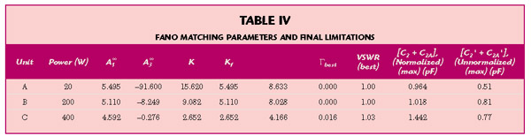
Note that for unit C, unlike the other units, the value in the last column is less than the existing built-in load capacitance (see the last column of Table 2), indicating that the latter is already limiting the best attainable reflection. This confirms the signal given for this unit by the fact that its K is less than its A1 8, and that an optimal matching circuit would therefore have to include an all-pass of the form previously shown in Figure 4 circuit c . At this point, its previously noted tutorial purpose having been accomplished, further analysis of unit C is abandoned and efforts to determine practical matching circuits for the remaining devices will proceed.
MATCHING WITH A FINITE NUMBER OF ELEMENTS
Recall that the above analysis established limitations only for an infinite number of matching elements, whereas space and tolerance considerations rarely permit more than two or three. Fano5 presents curves for the minimum attainable reflection of networks matched with varying finite numbers of elements, while Matthaei et al7 provides the optimum values of those elements for as many as four total reactances. Table 5 lists these optimum normalized and un-normalized values for 3 and 4 (total, including load) reactive elements (N is the number of elements), as well as the expected worst-case reflections.

Although three-element matching is seen to be sufficient to meet the specification for both units, four-element matching values are also shown for unit B. This is because actual devices must have an input tab (to connect to the external circuit trace) whose width and thickness may produce a capacitance/unit length exceeding that of a 50 W line on the termination substrate; this excess capacitance can often be taken up in C'4 . It may also be noted from the table that the optimum source impedance is not necessarily 50 W . Alternately interpreted, a 50 W source impedance will not necessarily have 50 W as the optimum load impedance. However, since the performance is well within specification and the indicated differences here are small, they shall be ignored.
Figure 5 shows the new Smith Chart reflection plots of the matched terminations. The maximum VSWR of the 20W unit has been reduced from 1.25 to 1.07; the VSWR of the 200W unit has been reduced from 1.47 to 1.04. Departure from the best theoretical performance shown in the table is assumed to result from inability to read the graphs in Matthaei7 to sufficient precision, plus the decision noted above to retain a 50 W load impedance. In both cases, it should be observed that predicted performance is well within specification.

FINAL MATCHING
The final steps in matching include realization of the appropriate lumped elements by distributed approximations. These are covered in Matthaei7 , Chapter 7, and are, in general, well known to practicing microwave engineers. Typically, the inductors are realized by narrow (high characteristic impedance) line segments, and the capacitors by sections of wide (low characteristic impedance) lines. After this has been done, a CAE program may be used to check and optimize results, taking into account various discontinuity reactances (such as occur when going from wide to narrow lines) that have herein thus far been ignored. At this point a hitch arises: To protect the surface of the termination from environmental and processing hazards, it must be covered, and the cover's electrical effect accounted for. Typical covers are made of 20-mil-thick 96 percent alumina, cemented to the termination's top surface by a thin layer of high-temperature epoxy. Generally, available CAD circuit models do not include the effects of such two-dielectric covers (creating so-called "embedded microstrip") as parametric inputs. Therefore, to make final design adjustments, as well as to verify the validity of some of the earlier assumptions, an electromagnetic model must be constructed, using software such as Genesys 7 3 or Sonnet ,8 which employ method-of-moments or method-of-lines approaches to achieve accurate solutions.
LAST STEPS
When an optimum design has been obtained and the circuit elements adjusted to conform to the EM model, a production yield study is accomplished by assigning tolerances and statistical distributions to all physical dimensions; substrate and cover dielectric constants and loss tangents; and film resistivity -- and then once more using software5 to perform a Monte Carlo analysis. As a practical matter in production, the final DC resistance will often have to be trimmed to value; some manufacturers use a laser to accomplish this by cutting notches in the film. However, care must be exercised here since the resultant current concentrations along the edges of the notch can result in local hot spots and consequent burn out under RF high power test conditions. To avoid this certain proprietary trimming techniques are available that do not require notching the film.
It should be noted that only terminations that are required to perform at frequencies down to DC have been of concern. If this constraint is relieved and the bandwidth limited, then Fano's relations in Equation 7 show that performance could substantially improve. Improvement would be accomplished by band-pass matching elements, for example, replacing inductors by series-resonant circuits and capacitors by shunt-resonant circuits. Such designs are beyond the scope of this discussion.
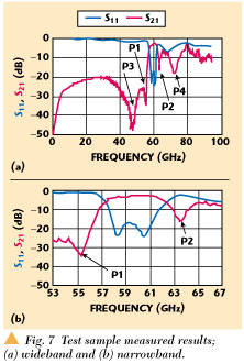
Figure 6 shows a 100 W AlN chip termination with the cover removed. The LC matching elements are the narrow line leading to the resistive film and the widened land to which a silver-plated beryllium copper tab is attached using lead free solder. Maximum VSWR is specified as 1.15 from DC through 4 GHz, though performance of a typical device, as shown in Figure 7 , which represents the average of data taken on eight randomly selected production units -- is substantially better over most of the range. This model has a sputtered (thin-film) wraparound, negating the need for separate screening and firing of an additional thick-film conductor and thereby increasing reliability. Temperature stability of the finished termination is augmented by a stabilization bake cycle.

CONCLUSION
Design considerations have been discussed for high power chip terminations, with emphasis on establishing fundamental thermal and electrical performance criteria and basic impedance-matching parameters. The design steps, illustrated with several examples, are: Compute the required resistive film area to meet the thermal requirements; check that the film is electrically thin (though physically thick) so that it will appear as a constant resistance over the frequency range of interest; calculate the element values of a two-term lumped approximation to the film's behavior and check that the approximation error is small; use Fano's impedance matching theory to establish ultimate reflection limits and matching network topology; use a standard matching network design to determine first-cut element values; improve the design by using a CAD circuit program to account for microstrip discontinuity reactances and an EM analysis program to account for cover and other effects not readily modeled and adjust the lumped circuit element values accordingly; and finally, use a CAD program to perform a Monte-Carlo production yield analysis. These steps will assure a final product that achieves the best possible performance consistent with physical constraints.
ACKNOWLEDGMENT
The author wishes to thank Mike Giacalone, David Liu, Gene McGuiness, Joe Tierney and Kate Levine for their assistance in the preparation of this article, and particularly, Allan Reynolds, for his thoughtful suggestions and critique. Victor Insetta created the technological environment that permitted this work to be accomplished.

References
1. S. Ramo and J. Whinnery, Fields and Waves in Modern Radio , John Wiley & Sons Inc., New York, 1953, pp. 251?253.
2. B. Wadell, Transmission Line Design Handbook , Artech House, MA, 1991, pp. 93?95
3. Genesys 7 , Eagleware Inc., Norcross, GA.
4. H.W. Bode, Network Analysis and Feedback Amplifier Design , Sec. 16.3, New York, Van Nostrand, 1945.
5. R.M. Fano, "Theoretical Limitations on the Broadband Matching of Arbitrary Impedances," Journal of the Franklin Institute , Vol. 249, January February 1950, pp. 57?84 and 139?154.
6. G.L. Matthaei, "Synthesis of Tchebycheff Impedance-matching Networks, Filters, and Interstages," IRE Transactions on Circuit Theory , September 1956, pp. 163?172.
7. G.L. Matthaei, L. Young and E.M.T. Jones, Microwave Filters, Impedance-matching Networks and Coupling Structures , McGraw Hill, New York, 1964, pp. 120?135.
8. Sonnet ,© Sonnet Software Inc., Liverpool, NY.
 Robert Grossbach received his BEE degree from Cooper Union in 1962 and the MSEE degree from Columbia University in 1965. Since 1962 he has worked on the development of microwave components and subsystems, both active and passive. He has also authored a number of novels, short stories and technical articles. He is currently the manager of RF Development Engineering at American Technical Ceramics, where his responsibility focuses on the characterization and development of ceramic-based RF components.