The most advanced commercial satellites transmit data down to Earth at rates of 100 to 200 Mbps; some advanced larger single satellite concepts target 1 to 4 Gbps. These data rates are substantially limited by state-of-the-art RF power amplifiers used to make the transmitters. Akash is building, for the first time, a small satellite system (12U) that will exhibit a preliminary downlink data rate of 14 Gbps. The next demo will feature data rates of over 100 Gbps. The ultimate technical goal is to demonstrate a downlink data rate of 1 Tbps from a single, modest size satellite—using GaN on Diamond RF power amplifiers.
GaN on Diamond
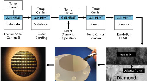
Felix Ejeckam, co-founder of Akash Systems Inc., invented GaN on Diamond in 20031 as a way to extract heat effectively from the hottest locations in a GaN transistor. The basic concept is that a cooler GaN amplifier would make the system more energy efficient, and less wasteful. On a GaN on Diamond wafer, the GaN channel or epitaxy is extracted from its original substrate of Si and situated on a CVD diamond substrate via a 35 nm SiN interfacial layer. This nanometer-scale proximity of a 200°C GaN channel to CVD diamond, the most thermally conductive industrial material, drastically reduces the thermal rise between the amplifier’s base plate and the channel temperature. Figure 2 shows the process of making GaN on Diamond wafers and devices. Many parties over the years have quantified the aforementioned thermal improvement.2 A GaN on Si HEMT wafer is bonded to a temporary Si carrier. The original Si substrate is etched away, followed by CVD deposition of diamond via a 35 nm interfacial layer below the GaN. Finally, the temporary Si carrier is etched away. The eventual GaN on Diamond wafer is then processed into an array of HEMTs or MMICs.

Figure 2 GaN on Diamond wafer process.

Figure 3 Example device shows 61 percent PAE from a 2.9 W (5.6 W/mm) HEMT with 7.9 dB gain. Bias point is 24 V.
System Impact
If the thermal rise of a GaN MMIC can be shrunk by 40 to 50 percent compared to GaN on SiC, then greater power density can be squeezed into a smaller volumetric space.3 Power is a direct parameter in a satellite’s downlink data-rate budget calculation; more information can be transmitted if there is more power. Cooling requirements in a very compact space are relaxed with GaN on Diamond since the ambient temperature can be allowed to rise higher than with a typical GaN on SiC power amplifier system—without compromising performance or reliability. This reduction in cooling gear also means less weight and size, both key parameters in the cost of launching a satellite system into orbit.
Performance
Akash designers have recently demonstrated high performing GaN on Diamond transistors (i.e., simplified power amplifiers) at K-Band exhibiting 60 percent power added efficiency (PAE) at 20 GHz (see Figure 3). In another recent work, funded by DARPA and performed by a team of researchers at Georgia Tech, Stanford, UCLA and Element Six, the GaN device’s thermal rise—change in temperature from the GaN channel to the substrate bottom—was found to reduce by 80°C when compared to the same device on GaN on SiC.2 The wafer used in the work is identical to the GaN on Diamond process used by Akash Systems.

Figure 4 Graph showing the temperature distribution for the channels from the center to the edge of the 10 finger HEMT for various types of GaN on Diamond wafers.
Figure 4 shows the temperature distribution for the channels from the center to the edge of the 10 finger HEMT for various types of GaN on Diamond wafers. Akash Systems uses the “Gradient Diamond with Low Thermal Boundary Resistance (TBR)” process GaN on Diamond wafers (in green); this curve registers 152°C peak temperature (the first peak). GaN on SiC registers 232°C at the same point on the device.2
Akash Systems is planning to launch into a LEO orbit in 2019, a 24 kg 12U (36 cm x 24 cm x 23 cm) satellite system that will contain a 20 W transmitter radio built on a GaN on Diamond power amplifier. The system will exhibit a landmark 14 Gbps data rate unique for a system that size.n
References
- F. Ejeckam, D. Francis, F. Faili, D.J. Twitchen, B. Bolliger, J. Felbinger and D. Babic, “S2-T1: GaN on Diamond: A Brief History,” Lester Eastman Conference on High Performance Devices, August 5–7 2014, DOI: 10.1109/LEC.2014.6951556. INSPEC Accession Number: 14775316.
- L. Yates, A. Sood, Z. Cheng, T. Bougher, K. Malcom, J. Cho, M. Asheghi, K. Goodson, M. Goorsky, F. Faili, D.J. Twitchen and S. Graham, “Characterization of the Thermal Conductivity of CVD Diamond for GaN on Diamond Devices,” Compound Semiconductor Integrated Circuit Symposium (CSICS) 2016 IEEE, pp. 1–4.
- G.D. Via, J.G. Felbinger, J. Blevins, K. Chabak, G. Jessen, J. Gillespie, R. Fitch, A. Crespo, K. Sutherlin, B. Poling, S. Tetlak, R. Gilbert, T. Cooper, R. Baranyai, J.W. Pomeroy, M. Kuball, J.J. Maurer and A. Bar-Cohen, “Wafer-Scale GaN HEMT Performance Enhancement by Diamond Substrate Integration,” 10th International Conference on Nitride Semiconductors, August 25-30, 2013, Washington, D.C.
