
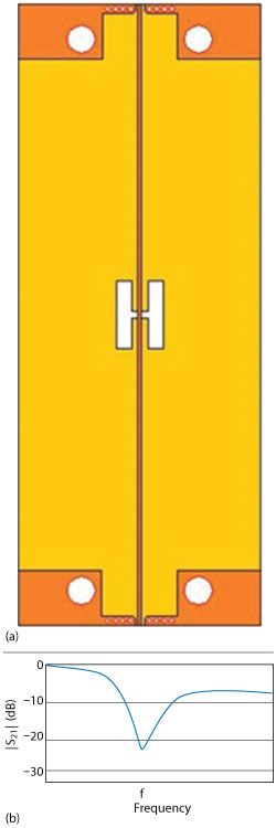
Figure 1 Top view of a microstrip transmission line with an H-shaped DGS etched in its ground plane (a) and |S21| for this structure (b).
A multilayer circuit design using defected ground structures is used to enhance filter performance without concern for leakage and isolation.
Microstrip defected ground structures (DGS) have been a part of high frequency circuit design for many years and are also used with stripline and coplanar waveguide circuits.1-3 While DGS circuit design approaches can provide benefits in the performance and miniaturization of resonator-based RF/microwave components, such as antennas and filters, the technology is limited by serious drawbacks, including low isolation and excess electromagnetic (EM) radiation. DGS-based circuits can radiate EM energy, resulting in electromagnetic interference. Lack of isolation can also result in undesirable interaction with neighboring RF/microwave components and circuits. Fortunately, because of the increasing use of multilayer circuit configurations in modern RF/microwave circuit designs, it is possible to design and fabricate microstrip DGS circuits with little or no concern for radiation or isolation. This multilayer approach is demonstrated with a lowpass filter (LPF) design and some readily available commercial circuit materials.
DGS OVERVIEW
Perhaps the easiest way to understand a DGS is to consider a ground plane as a continuous structure, with no breaks or interruptions. The electrical characteristics of a transmission line, such as microstrip, assumes this ground plane continuity. By purposely forming a defect, such as an isolated opening etched in the ground plane, the transmission line’s RF characteristics are altered. Capacitance and inductance can change significantly in the area of the DGS.
A simple example is an H-shaped feature etched in the ground plane of a microstrip transmission line (see Figure 1). The microstrip structure shown in Figure 1a has two copper layers. The dark orange color represents circuit features on the top copper layer (the signal layer), and the light orange color depicts circuit features on the bottom copper layer (the ground plane). The H-shaped DGS produces a bandstop or band-reject characteristic, as shown in Figure 1b. The response is similar to a one-pole Butterworth lowpass filter (LPF). The DGS pattern can be altered to generate a very narrowband bandstop response, which is sometimes added to a filter design to improve isolation in the stopband portion of the filter. As will be shown with a practical LPF design, the effective use of a microstrip DGS not only improves a filter’s stopband response but greatly improves a filter’s spurious harmonic responses.
A DGS can enhance the performance of many RF/microwave components, including LPFs, bandpass filters (BPF), patch antennas and other resonant circuits. A search of the IEEE Xplore® Digital Library yields many white papers where a DGS is used in these applications. DGS structures can also be used to reduce circuit size, with the ability to implement slow-wave effects.
OVERCOMING DGS RADIATION AND ISOLATION
With the growing complexity and integration found in modern RF/microwave circuits, multilayer circuit construction is often employed. Proper design of a multilayer printed circuit board (PCB) circuit containing a microstrip DGS can minimize or even eliminate EM radiation and isolation. Multilayer PCBs can be constructed in many shapes and sizes.
For the sake of simplicity, a multilayer PCB with three copper layers is used as an example to demonstrate a method for minimizing DGS radiation and isolation (see Figure 2). The figure shows a multilayer PCB with two different substrate materials having dielectric constants εr1 and εr2. For an ideal DGS, the dielectric constant of the lower substrate material, εr2, is a value equivalent to that of air, i.e. εr2 = 1.0. It is possible to embed an air cavity within a multilayer PCB, but it is difficult and typically expensive to fabricate. A compromise is to use a substrate with a low value of εr2 that is robust enough to tolerate PCB manufacturing processes. The benefits of using substrate materials with different εr values are explained later in this article.4,5
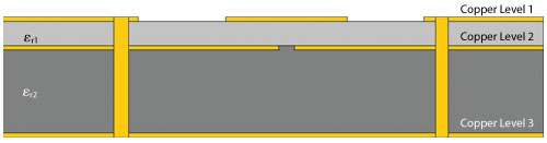
Figure 2 Cross-section of a PCB with three copper layers used to realize a microstrip DGS without radiation and isolation concerns.
The top two copper layers are microstrip and its defected ground plane. They may appear as grounded coplanar waveguide transmission lines, but they are actually loosely coupled to behave as microstrip. The use of ground planes with plated-through-holes (vias) connecting all three ground layers ensures that the system ground connects the top and bottom ground planes and provides a suitable connection to the buried microstrip (defected) ground plane on copper layer 2. Proper grounding of this buried layer is essential for optimum microstrip and DGS performance. For a traditional microstrip DGS structure with two copper layers, the ground plane with the DGS opening can radiate energy to the nearby environment. However, with the multilayer construction shown in Figure 2, the radiated energy is captured within the circuit, due to the ground on copper layer 3 and its repetitive grounding vias.