A wideband high efficiency Doherty power amplifier (DPA) that works in the 1.85 to 2.4 GHz band (26 percent fractional bandwidth) employs two pairs of anti-coupled lines with stepped impedance resonators to replace the λ/4 transmission lines in a conventional DPA for harmonic suppression and phase compensation. Maximum output power is between 43.0 and 44.1 dBm. At 6 dB output power back-off (OPBO), the maximum drain efficiency (DE) is 61.3 percent, with gain higher than 12 dB. In the saturated output power region, the efficiency is between 67 and 76.6 percent with gain higher than 8 dB. Compared with a conventional DPA, the third-order intermodulation distortion (IMD3) is reduced by 22 dB while efficiency and gain performance are greatly improved.

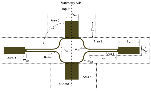
Figure 1 Phase compensation structure for the Doherty power amplifier.
In wireless communication basestations, Doherty power amplifiers1 are widely used to provide high efficiency in the presence of modulated signals with high peak to average power ratios. The λ/4 transmission line in a conventional DPA is used mainly to perform impedance matching and provide phase delay compensation. The fractional bandwidth is typically narrow (usually less than 10 percent), because the λ/4 transmission line can achieve an optimum impedance transformation and phase compensation only at one frequency. This limits its application in multiband, multi-standard base stations. Moreover, the peaking amplifier in the DPA operates class C, and as a result, has relatively poor linearity.

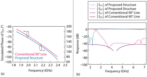
Figure 2 Simulated performance of the phase compensation structure vs. a conventional 90° line: ∠ S21 (a), |S11| and |S22| (b).

The λ/4 transmission line in a conventional DPA also exhibits weak harmonic suppression. Some strategies to address this, like composite right/left-handed transmission lines (CRLH-TL), defected ground structures (DGS), analytical model simplification and harmonic tuning, have been successfully reported.2–5 Fang and Quaglia2 report a DPA with 18 percent fractional bandwidth; however, the DE and gain at 6 dB OPBO are only 36 percent and 6 dB, respectively. For comparable linearity, CRLH-TL and DGS were adopted with the standard DPA topology for a power-added efficiency (PAE) at 6 dB OPBO of about 20 percent.3,4 Zhao et al.,5 report on a similar case with measured results showing less obvious improvement in linearity by utilizing a simple analytical model. A 35 percent fractional bandwidth is reported by Bathich et al.,6 by exploiting wideband filters; in this case, a standard topology is also adopted, but the Doherty behavior is not clearly demonstrated. Sarkeshi et al.,7 employ frequency reconfigurable matching networks enabling a fractional bandwidth of about 20 percent; however, this requires an external control circuit.
In this work, a compact phase compensation architecture based on two pairs of anti-coupled lines loaded with stepped impedance resonators replaces the λ/4 transmission line in a conventional DPA. This structure performs impedance conversion, phase compensation, phase correction and harmonic suppression. At the same time, it provides an easy way to tune performance by adjusting the width and length of the stepped impedance resonators.

Figure 3 Block diagram (a) and fabricated (b) DPA.
PHASE COMPENSATION NETWORK
Even/odd mode analysis was used to analyze the axially symmetric novel and compact DPA structure shown in Figure 1. First analyzed is the two-port network in area 1. Zoe and Zoo represent the even mode and odd mode characteristic impedances of the parallel coupled line. [ZU], [ZD] and [ZT] represent the impedance matrices of the parallel coupled line, the low impedance line and the two-port network in area 1, respectively. The impedance matrix of the two-port network is given by8,9


Figure 4 Measured and simulated power gain vs. output power (a) and frequency, at 6 dB OPBO and saturation (b).
θe and θo represent the even and odd mode electrical lengths, respectively. From the relation between the ABCD matrix and the impedance matrix,9 we derive the ABCD matrix of the two-port network. The physical length of the microstrip curved line in area 2 is designated l and the ABCD matrix of the two-port network is designated [MH]. These are given as follows,

The networks in areas 2 and 3 are symmetric and have a parallel relationship. [MF] represents the ABCD matrix of the two-port network that consists of the structures in areas 2 and 3. By analyzing the relation between voltage and current of the two-port networks of areas 2 and 3, [MF] is given as follows,

Figure 5 Measured and simulated output power vs. input power (a) and saturated output power vs. frequency (b).

AH, BH, CH and DH are defined in Equation 2.
The input microstrip line in area 5, the output microstrip line in area 4 and the parallel network of areas 2 and 3 have a cascade relationship. With [MG] representing the ABCD matrix of the entire structure and [MK] representing the input microstrip line in area 5, [MG] is given as

From the relationship between the ABCD matrix and the scattering matrix,9 the scattering parameters of the structure are


φ21, φ11 and ψ21 are the phase of S21, S11 and Z21, respectively. AG, BG, CG and DG are given in Equation 5. Using design specifications for |S21|, |S11|, |Z21| and φ21 and Equations 6–8, a compact phase compensation architecture based on two pairs of anti-coupled lines with stepped impedance resonators is implemented.

Figure 6 Measured and simulated drain efficiency vs. frequency at 6 dB OPBO and saturation (a); measured drain efficiency vs. output power vs. frequency (b).
Figure 2 shows its simulated performance. The simulated transmission phase of the structure is shown in Figure 2a, while the magnitude of the S-parameters is shown in Figure 2b. Figure 2b shows that the conventional λ/4 transmission line provides almost 0 dB harmonic suppression, while second harmonic suppression is better than 40 dB and third harmonic suppression is about 30 dB in the new structure. Table 1 shows the characteristic impedance of the structure, which is around 50 Ω. A compact structure implemented by capacitor-loaded coupled lines is reported by Li et al.,8 but its second and third harmonic suppression is only about 20 dB. Zhang et al.,10 report on a structure consisting of a pair of anti-coupled lines short circuited by a low impedance line; however, second and third harmonic suppression are also limited to around 20 dB.
REALIZATION AND CHARACTERIZATION
To verify this design, a DPA operating over a 1.85 to 2.4 GHz band was realized. It is fabricated on a Taconic substrate with copper metallization (RF35 with a relative dielectric constant εr = 3.5, substrate height h = 0.508 mm, metal thickness t = 0.035 mm and loss tangent tan δ = 0.0018). The main and peaking power amplifiers are implemented with Cree CGH40010F GaN HEMTs.
Figure 3 shows the block diagram and photo of the implemented DPA, respectively. A Wilkinson power divider splits the input power equally. The location of the phase compensation structure is indicated in Figure 3a. The dimensions of the DPA are approximately 1.5 λg × 1 λg, where λg is the guide wavelength at center frequency f0 = 2.125 GHz.
Measurements were taken in 50 MHz steps with single-tone CW excitation. The main PA operates class A/B with VDS = 28 V and VGS = ‐2.5 V (Id = 210 mA). The peaking PA operates class C with VDS = 28 V and VGS = ‐3.7 V. Measured and simulated power gain as a function of output power are shown in Figure 4. Differences between measurement and simulation at low and moderate output power are attributed to simplifying assumptions used in the model for the PA output load impedance. Saturated gain is higher than 8 dB, as shown in both measurement and simulation. Figure 4b shows measured and simulated gain as a function of frequency at 6 dB OPBO and in saturation. Gain at 6 dB OPBO is higher than 12 dB in the 1.85 to 2.4 GHz band. Gain flatness is similar at 6 dB OPBO or when saturated. Figure 5a shows the measured and simulated output power as a function of input power at 1.85, 2.1 and 2.4 GHz. Saturated output power over frequency is shown in Figure 5b; the saturated power is between 43 and 44.1 dBm.

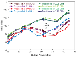
Figure 7 Measured IMD3 performance vs. output power, comparing the coupled line design with a conventional Doherty.
The DE at saturated output power and 6 dB OPBO as a function of frequency and output power are shown in Figures 6a and 6b, respectively. The DE at saturation is between 67 and 76.6 percent, and the drain efficiency at 6 dB OPBO is between 35 and 61.3 percent. Measured and simulated DE at saturation are comparable; however, the drain efficiency at 6 dB OPBO shows some differences from the simulated results. This is due mainly to the influence of fabrication tolerances.
Figure 7 shows the measured IMD3 of the DPA based on this work versus a conventional DPA, using two tones spaced 6 MHz apart, at 1.85, 1.90, 2.08 and 2.15 GHz. The IMD3 is improved by about 22 dB at high-power compared to the conventional DPA. In the region where output power is higher than 30 dBm, the best IMD3 is ‐44 dBc at 2.08 GHz. IMD3 performance is improved across the board. Note the rise in IMD3 as the output power is increased above 38 dBm. This is because the peaking amplifier is completely turned on, generating more third-order intermodulation.
DPA performance from this work is compared with other reported results in Table 2.4,11-13 Several DPAs with fractional bandwidths higher than 30 percent are shown, but their saturated efficiencies and efficiencies at 6 dB OPBO are lower. The DPA described by Sun and Jansen12 achieves a bandwidth higher than 30 percent, but its best IMD3 is only ‐35 dBc at high-power.

CONCLUSION
A compact phase compensation architecture based on two pairs of anti-coupled lines loaded with stepped impedance resonators replaces the λ/4 transmission line in a conventional DPA. Compared to a conventional DPA, this design demonstrates an improvement in efficiency, gain and IMD3.n
References
- W. H. Doherty, “A New High Efficiency Power Amplifier for Modulated Waves,” Proceedings of the Institute of Radio Engineers, Vol. 24, No. 9, September 1936, pp. 1163–1182.
- J. M. Rubio, J. Fang, V. Camarchia, R. Quaglia, M. Pirola and G. Ghione, “3 to 3.6 GHz Wideband GaN Doherty Power Amplifier Exploiting Output Compensation Stages,” IEEE Transactions on Microwave Theory and Techniques, Vol. 60, No. 8, August 2012, pp. 2543-2548.
- Y. C. Jeong, S. G. Jeong, J. S. Lim and S. Nam, “A New Method to Suppress Harmonics Using Bias Line Combined by Defected Ground Structure in Power Amplifiers,” IEEE Microwave and Wireless Components Letters, Vol.13, No.12, December 2003, pp. 538-540.
- S. H. Ji, S. K. Eun, C. S. Cho, J. W. Lee and J. Kim, “Linearity Improved Doherty Power Amplifier Using Composite Right/Left-Handed Transmission Lines,” IEEE Microwave and Wireless Components Letters, Vol. 18, No. 8, December 2008, pp. 533–535.
- Y. Zhao, A. G. Metzger, P. J. Zampardi, M. Iwamoto and P. M. Asbeck, “Linearity Improvement of HBT-Based Doherty Power Amplifiers Based on a Simple Analytical Model,” IEEE Transactions on Microwave Theory and Techniques, Vol. 54, No. 12, December 2006, pp. 4479–4488.
- K. Bathich, A. Markos and G. Boeck, “A Wideband GaN Doherty Amplifier With 35 Percent Fractional Bandwidth,” Proceedings of the European Microwave Conference, September 2010, pp. 1006-1009.
- M. Sarkeshi, O. B. Leong, and A. van Roermund, “A Novel Doherty Amplifier for Enhanced Load Modulation and Higher Bandwidth,” IEEE MTT-S International Microwave Symposium Digest, June 2008, pp. 763–766.
- R. Li, D. I. Kim and C. M. Choi, “Compact Structure With Three Attenuation Poles for Improving Stopband Characteristics,” IEEE Microwave and Wireless Components Letters, Vol. 16, No. 12, December 2006, pp. 663–665.
- D. M. Pozar, Microwave Engineering, 3rd ed., Wiley, N.Y., 2005.
- J. Zang, L. Li, J. Gu and X. Sun,“Compact and Harmonic Suppression Wilkinson Power Divider With Short Circuit Anti-Coupled Line” IEEE Microwave and Wireless Components Letters, Vol. 17, No. 9, September 2007, pp. 661-663.
- L. Piazzon, R. Giofrè, P. Colantonio and F. Giannini, “A Wideband Doherty Architecture With 36 Percent of Fractional Bandwidth,” IEEE Microwave and Wireless Components Letters, Vol. 23, No. 11, November 2013, pp. 626-628.
- G. Sun and R. H. Jansen, “Broadband Doherty Power Amplifier Via Real Frequency Technique,” IEEE Transactions on Microwave Theory and Techniques, Vol. 60, No. 1, January 2012, pp. 99-111.
- S. Watanabe, Y. Takayama, R. Ishikawa and K. Honjo, “Miniature Broadband Doherty Power Amplifier With a Series-Connected Load,” IEEE Transactions on Microwave Theory and Techniques, Vol. 63, No. 2, February 2015, pp. 572-579.
