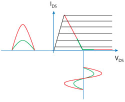
Figure 1 Simple class AB amplifier load line.
A modified three-level Doherty amplifier produces good efficiency over 10 dB of operation using devices of equal periphery. Test results are presented that demonstrate a drain efficiency of greater than 40 percent at 10 dB back-off.
Modern communication systems routinely use complex modulation techniques that result in peak-to-average ratio (PAR) signals of 9 dB and higher. To achieve sufficient linearity, these high PAR levels require a power amplifier (PA) to operate far below the power levels that would yield optimum power-added efficiency. To understand this effect, consider one of the simplest forms of an RF amplifier, the class AB type shown in Figure 1.
Such an amplifier is relatively straightforward to design and manufacture and can easily provide peak drain efficiencies of around 65 percent when operating in the 2 GHz region. One drawback with this type of simple amplifier is that when the RF output signal level is reduced, the output voltage swing decreases and efficiency drops with the square root of the output power. This means that at a quarter of the output power (-6 dB), efficiency is about half of what it is at peak output power, or 32 percent in this example. Clearly, operating at 6 dB back-off and higher with a class AB amplifier results in a significant reduction in efficiency, because the signal is, on average, sitting at a highly inefficient operating point.
The use of a Doherty amplifier is a well known technique for improving efficiency of a PA in backed-off operation. The standard two-way Doherty amplifier with a peak in efficiency at 6 dB back-off and full power is commonly used and well understood. With the use of increasingly complex signals comes the challenge to move the peak in efficiency to higher levels of back-off while maintaining efficiency up to full power output. This can be achieved with asymmetrical Doherty amplifiers or by utilizing N-way Doherty techniques. This is why the use of Doherty amplifiers in modern code division multiple access (W-CDMA) and long-term evolution (LTE) systems has seen a strong resurgence.
The two-way Doherty amplifier provides an improvement over class AB operation, but with higher levels of PAR being used it is necessary to improve efficiency at back-off levels of 10 dB and higher. The three-level or three-way Doherty amplifier produces peaks in efficiency at 9.5, 4.4 and 0 dB, which is a good fit for LTE transmitters. However, as will be seen later, the conventional approach requires that the two auxiliary amplifiers be twice the periphery of the main amplifier.

Figure 2 Single-ended class AB amplifier (a) and two-way Doherty amplifier (b).
This article describes the operation of a modified three-level Doherty amplifier1 that produces good efficiency over the top 10 dB of operation using devices of equal periphery. Its operation is explained based on an Ampleon (formerly NXP) design that uses three laterally diffused metal oxide semiconductor (LDMOS) transistors of equal size. Design challenges faced with this type of amplifier are presented and compared against the conventional three-way Doherty architecture. Test results are presented that demonstrate a drain efficiency of greater than 40 percent at 10 dB back-off.
The entire RF design, including layout, is implemented in the NI AWR Design Environment. Within this software environment, Microwave Office circuit design software and APLAC harmonic balance are used to simulate, in detail, the large-signal effects of the Doherty amplifier’s operation. The software’s load-pull analysis is used to determine the impact of load impedance on amplifier performance.
Two-Way Doherty Design
Although well documented in the literature, it is worth taking a moment to revisit the simple case of the two-way Doherty amplifier to fully understand the three-level configuration. The standard two-way Doherty amplifier works by splitting the amplifier into two equally-sized amplifiers that are half the size of a single-ended class AB amplifier with the same peak power capability (see Figure 2). The basic principle is that when the output signal level is low, only the main amplifier is active. With increasing output levels, the auxiliary amplifier is progressively introduced up to the point where full power is achieved, and both the main and auxiliary amplifiers contribute equally to deliver full power.

Figure 3 Theoretical efficiency of a two-way Doherty amplifier.
The two-way circuit is configured with the main amplifier biased in class AB and the auxiliary amplifier biased in class C. This biasing scheme means that at low input drive levels, the main amplifier conducts and the auxiliary amplifier is off. As input levels are increased, the main amplifier drive level also increases. When the output power is a quarter (‐6 dB) of the amplifier maximum, the auxiliary amplifier starts to conduct current. At low signal levels, when the auxiliary amplifier is not active, the main amplifier (assuming RL = 25 Ω) “sees” 100 Ω. This means that it reaches full voltage swing at half power. Full voltage swing means that the main amplifier provides maximum efficiency at half its output power. At this point, the amplifier, as a whole, is delivering a quarter (‐6 dB) of its peak power capability with maximum efficiency. This is the first point on the theoretical efficiency curve in Figure 3.
As input drive level is increased from the 6 dB back-off point, the current contribution into the load from the auxiliary amplifier increases. This increased current injected by the auxiliary amplifier means that the impedance looking into the load increases. The 50 Ω impedance inverter between the load and the main amplifier ensures that the main amplifier sees a reduced load as the current contribution from the auxiliary amplifier increases. So, in this regime, as output power increases, there are two processes taking place. The first is that, due to load modulation from the auxiliary amplifier, the main amplifier is effectively increasing in size; that is, its capability to produce power is increasing during the time it is running at maximum voltage swing and hence maximum efficiency. The other process taking place is that both the main and auxiliary amplifiers contribute to the total output power.

Figure 4 Standard two-way Doherty load modulation with the inverter removed.
As the drive level increases further, these processes continue to increase until the auxiliary amplifier is at maximum output power (if the devices are equal in size) and the currents into the load from the main and auxiliary amplifiers are equal. At this point the main and auxiliary amplifiers both see 50 Ω. The key concept in the operation of the Doherty amplifier is load modulation. The explanation given by Cripps2 provides an excellent description of the principles involved. The key elements are summarized here for clarity.
Figure 4 represents the simplest possible case where two current sources are feeding into a common load. When I2 = 0, the impedance Z1 is simply equal to RL. If a current is injected into the load from I2 then the impedance Z1 is modified to:

If I1 and I2 are equal, then Z1 = Z2 = 2RL. With the addition of an impedance inverter as shown in Figure 5, this circuit becomes the two-way Doherty. The addition of the inverter causes the impedance seen at the main amplifier, Zm, to decrease when the current from the auxiliary amplifier is injected into the common load. When the auxiliary amplifier is off Zm = Zo2 /RL.

Figure 5 Two-way Doherty amplifier.
Conventional Three-Level Doherty Design
As shown in Figure 6, the conventional three-level Doherty amplifier is a direct extension of the two-way design. By adjusting the relative device periphery between the main and auxiliary amplifiers, it is possible to achieve a variety of different positions for the efficiency peaks. The designer can use the equations defined by Edmund, et al.3 to locate the efficiency peaks as required. This article is concerned with signals around 10 dB of PAR. The relative levels of device periphery to achieve an efficiency peak at ‐9.5, ‐4.4 and 0 dB for the conventional three-level Doherty is 1:2:2, where the first digit is the main amplifier followed by Aux 1 and Aux 2.
For this configuration, Z01 is required to be 70.7 Ω, Z02 = 33.3 Ω and RL = 20 Ω. At the first efficiency peak, the main amplifier sees an impedance of 90 Ω. In order to match the output to 50 Ω, an impedance inverter with a value of √(20*50)=31.6 Ω is required. In essence, the conventional three-level Doherty amplifier behaves as a two-way Doherty amplifier up to the second peak (‐4.4 dB) in efficiency; then, from the second peak to full power, the main and auxiliary 1 amplifiers behave like a main amplifier that is load modulated by the current contribution from auxiliary 2.

Figure 6 Conventional three-level Doherty amplifier.
There are two main drawbacks to the conventional three-level Doherty amplifier. The first is that different device sizes are required to provide efficiency peaks in the 10 dB back-off region, which leads to added complexity. The second is that the load modulation of the main amplifier stops between the second and final efficiency peaks. This means that the main amplifier is driven into extreme saturation over the last 6 dB of output power.1
Modified Three-Level Doherty With Equal Devices
The modified three-level Doherty design1 achieves similar performance to a conventional three-level Doherty amplifier without having to accommodate output transistors of different sizes. Using transistors of equal size for the main and auxiliary stages has a number of practical benefits, including the use of a single “unit cell” RF design. The basic amplifier unit cell for the main and auxiliaries can be of the same (or very similar) design, which reduces development time. Also, having three of the same part rather than two different parts on the bill of materials results in economies of scale, which is important for what are likely to be the most expensive components in the amplifier. The configuration also provides proper load modulation of the main amplifier, whose load impedance is steadily reduced with increasing drive level. A schematic of the modified three-level Doherty is shown in Figure 7.

Figure 7 Modified three-level Doherty amplifier.

Figure 8 Theoretical efficiency of a three-way Doherty amplifier.
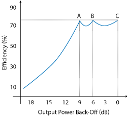
The best way to understand the operation is to start at low signal levels, progressively increasing the input drive and discussing the operation at each efficiency peak (see Figure 8). Each unit cell in this example delivers maximum output power when driving a 50 Ω load. The unit cell also contains phase offset lines to ensure that the electrical length of an auxiliary (and main) stage is 180 degrees from the active device at the point where the amplifier is connected into the Doherty combiner circuit. This ensures that when the auxiliary amplifier is switched off, an open circuit is presented to the Doherty combiner and minimum power is dissipated in the auxiliary output matching circuits. The main amplifier is biased in a class AB mode, auxiliary 1 is biased at about 0.7 V, and auxiliary 2 is biased at about 0 V when using enhancement mode LDMOS transistors. These values provide the required progressive switching of the auxiliary amplifiers. Note that the load is 16.7 Ω in this example and transformed up to 50 Ω with a 28.8 Ω quarter-wave inverter.
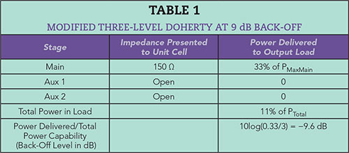
At low signal levels, in the regime before point A in Figure 8 is reached, only the main amplifier is active. The impedance presented to the main amplifier unit cell at this point is 150 Ω. At point A (9 dB back-off) the conditions shown in Table 1 apply. As the input drive level increases, it moves to the region between points A and B (6 dB back-off) in Figure 8. At point A, auxiliary 1 switches on and starts to deliver current into the common output load RL. This increase in current into the common load causes the impedance seen from the main amplifier at node A to increase. The action of the inverter Z01 in the main path causes the impedance seen by the main amplifier to fall. This reduction in output impedance enables the main amplifier to deliver more power into the common load while remaining in voltage saturation.

As drive level increases, this process continues until the current in the load due to the auxiliary amplifier is half the current in the load due to the main amplifier, and the following condition is reached:

This condition is point B in Figure 8 and is the second efficiency peak. Applying Equation 1, the impedance seen from the main amplifier looking into node A is given by:

So, the impedance seen by the main device looking into the 50 Ω inverter Z01 is 100 Ω. Also, the impedance seen from the auxiliary branch looking into node A is given by:

The impedance at node B looking from the auxiliary 2 amplifier is therefore 12.5 Ω (due to Z03), and the impedance seen by the auxiliary 1 unit cell amplifier is 200 Ω. Since the main and auxiliary 1 amplifiers are both running at voltage saturation, they both deliver maximum efficiency, hence the peak in efficiency. The amplifier parameters at this second efficiency peak are given in Table 2.

Bias of the auxiliary 2 amplifier is set such that it starts to turn on and deliver current into the output load when Equation 2 is satisfied. The increase in current further reduces the main impedance and allows it to deliver more power. The increased current into the load also reduces the load impedance seen by the auxiliary 1 amplifier, so this device delivers more power and further increases load current. This increase in current continues until the contribution from each amplifier is equal and the following is satisfied:

The two auxiliary amplifiers deliver a total normalized current of 2 into the load and the main amplifier delivers 1. This is point C in Figure 8. At this point, the impedance from the main branch looking into node A is now

The main amplifier sees 50 Ω and delivers full power. The impedance seen from the auxiliary branch looking into node A is given by:

Since Z03 is a 25 Ω inverter, the impedance looking into node B is also 25 Ω. This is the correct impedance for two 50 Ω loads in parallel. The parameters for the amplifier at this third and final efficiency peak (0 dB back-off) are given in Table 3.


Figure 9 Slipstream Engineering’s 2.14 GHz three-way Doherty amplifier.
In addition to the design of the output network, there are a number of practical design considerations for this type of amplifier that should be considered. The first is that the gain of the three-level amplifier is inherently quite low because of the three-way input split. This results in the small-signal gain being a minimum of 4.7 dB lower than that obtained from a single-ended device. This is less of an issue at lower cellular bands but can become a problem at higher frequencies, where gain is at a premium. The quarter-wave transformers used extensively throughout this design limit the bandwidth to about four to five percent maximum, so this approach is only applicable for narrowband applications.
Experimental Results
To demonstrate the concept, a 2.14 GHz version of the Ampleon three-level amplifier was designed and manufactured by Slipstream Engineering Design. A photograph of the amplifier is shown in Figure 9. The three-way input split (‐4.7 dB) is achieved by using a 5 dB directional coupler cascaded with a 3 dB hybrid coupler. The transistors used are twin LDMOS devices running at 28 V bias (normally used for push/pull or balanced applications) with one of the transistors unused in the upper device. Results are presented as back-off levels from the full output power of 150 W, which in this case is defined as about 2 dB output compression (see Figure 10). As can be seen, the design objective of 40 percent drain efficiency at 10 dB back-off is achieved over the band of interest. The small-signal gain of this amplifier is about 16 dB, with a power gain at full power of 14 dB.

Figure 10 CW drain efficiency vs. back-off vs. frequency. Full power is 150 W.
Conclusion
This article presented an overview and explanation of the operating principles for a modified Ampleon three-level Doherty amplifier3 that produces good efficiency over the top 10 dB of operation using devices of equal periphery. Design challenges faced with this type of amplifier were discussed and compared with those of a conventional three-way Doherty architecture. Experimental results demonstrate a drain efficiency of greater than 40 percent at 10 dB back-off.
References
- R. Gajadharsing, W. C. E Neo, M. Pelk, L. C. N. De Vreede and J. Zhao, “3-Way Doherty Amplifier With Minimum Output Network,” U.S. Patent US20100315162, issued December 16, 2010.
- S. Cripps, “RF Power Amplifiers for Wireless Communications,” Artech House, Norwood, Mass., April 1999.
- W. C. Edmund Neo, J. Qureshi, M. J. Pelk, J. R. Gajadharsing and L. C. N. de Vreede, “A Mixed Signal Approach Towards Linear and Efficient N-Way Doherty Amplifiers,” IEEE Transactions on Microwave Theory and Techniques, Vol. 55, No. 5, May 2007.
Mike Roberts is co-founder and technical director of Slipstream Design Engineering Ltd.

