
Cavity and Surface-mount Delay Line Filters for Feedforward Power Amplifiers
K&L Microwave Inc.
Salisbury, MD
In their quest for reduced levels of intermodulation distortion (IMD), power amplifier manufacturers utilize feedforward techniques to implement either multiple carrier power amplifiers or single wideband carrier power amplifiers. The feedforward technique relies on two feedback loops, which combine a portion of the distortion-free amplifier input signal with a portion of the distorted amplified output (sideband) signal. The fundamental carrier(s) of interest is nulled in the feedback loop so that the remaining signal contains only the distorted (sideband) energy. This signal is then amplified by an error amplifier and fed 180° out of phase directly to the amplifier’s output to null out the distorted sideband energy while preserving the fundamental carrier(s) energy. A basic block diagram for a typical feedforward scheme is shown in Figure 1 .
There are as many types of feedforward designs as there are applications that use them. However, one component common to feedforward designs is the mechanism that creates the delay in the primary high power and secondary low power portions of the feedforward loop. Historically, delay mechanisms have been provided through a predetermined length of coaxial cable in both the high and low power portions of the feedforward loop. There are several distinct advantages to using coaxial cable, including phase stability/deviation from linear phase vs. operating temperature and high power handling characteristics.
There are also significant disadvantages to coaxial cable, including large occupied volume, high insertion loss and grounding difficulties. To achieve 15 ns delay, approximately 10.5 feet (1.43 ns/ft.) of semirigid coaxial cable is needed. This long length requires > 15 in3 (0.141" diameter) or > 5 in3 (0.085" diameter) of PCB space to be dedicated to the coaxial cable. Depending upon the type of semirigid coaxial cable used, insertion loss can be relatively high. Using 0.11 dB/ft. for 0.141" diameter and 0.19 dB/ft. for 0.085" diameter semirigid cables, insertion loss at 1 GHz will be 1.2 dB and 2 dB, respectively. Loss increases to 1.7 and 2.8 dB, respectively, as the frequency increases to 2 GHz. Cable with a diameter of 0.047", while smaller and less expensive, introduces even higher loss and is extremely fragile, thereby complicating the manufacturing process.
In addition, the design engineer is often forced to incorporate additional (and costly) secondary manufacturing processes, such as hand soldering, or elaborate mechanical mounting methods to ensure proper grounding of the large and bulky coaxial cable delay assembly. Thus, a method that reduces the size, loss and grounding difficulties of the coaxial approach while retaining good phase stability/deviation from linear phase and high power handling characteristics would be advantageous.
Delay line filters are devices that provide these improvements. A filter-based delay line can be thought of as a wide bandpass filter with optimized group delay, deviation from linear phase and power handling over the specified band of interest that provides the delay function required by the feedforward circuit. The characteristics of the delay line filter can be specifically tailored to feedforward loop (high or low power) requirements. These types of delay line filters are currently available in cavity and surface-mount styles for enhanced performance in feedforward amplifier applications.
Cavity Delay Filters
A cavity (TEM mode) filter is typically required in the high power section of the  feedforward circuit. Power handling in this portion of the feedforward circuit is usually in the 50 to 100 W CW category, with peak instantaneous power as high as 1500 W. A cavity filter will reduce the amount of occupied space and insertion loss when compared to 0.141" diameter semirigid cable. Figure 2 shows the phase response and group delay vs. frequency of an all-pole TEM-mode cavity filter providing 15 ns delay over the 869 to 894 MHz AMPS BTS transmit band. Typically exhibiting 1.3 ns group delay variation and 1.7° p-p deviation from linear phase, this delay line filter will occupy a volume of only 7.5 in3 with an insertion loss contribution of 0.5 dB, representing 50 percent improvement in occupied volume and 0.7 dB insertion loss improvement over a 0.141" diameter coaxial cable type.
In addition to reducing the size of the amplifier, feedforward power amplifier manufacturers are able to take advantage of the reduced insertion loss a cavity delay filter offers by backing off the output power into a more linear region of operation (thus further reducing IMDs) or allowing increased output power. For the backoff option, IMDs are improved 3 dB (min) (6 dB, typ) for every 1 dB reduction in output power. The insertion loss savings provided by the cavity delay line filter provide an additional competitive advantage to the feedforward power amplifier manufacturer.
Cavity filters are simple to install and ground, thus eliminating the secondary processes and expense usually required with delay cables. Due to its wide bandwidth and low group delay variation, the inherent power handling of the 15 ns delay line filter exceeds 50 W CW and 500 W peak instantaneous without the need for special modifications. The filter could be modified for hundreds of watts CW and thousands of watts peak instantaneous power applied within its passband if required. This delay line filter is spurious free and provides rejection to at least the third harmonic, which simplifies the designer’s harmonic/spurious rejection requirements.
Note that design techniques to optimize delay flatness (such as cross-coupled resonators) have not been introduced into this example. Such techniques could appreciably improve the group delay variation to within ±0.1 ns (max) and deviation from linear phase response to 1° p-p (max) over the 869 to 894 MHz operating band. However, improving these specifications increases complexity and cost. Therefore, design engineers must carefully weigh the benefits against system application and cost goals. The decision will often depend upon the instantaneous bandwidth of the carriers to be applied to the amplifier’s input.
For example, if three IS-95 CDMA carriers are applied within a 5 MHz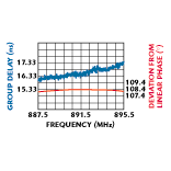 bandwidth in the 869 to 894 MHz operating band, the deviation from linear phase can be specified within any 5 MHz area over this band. Consequently, a simpler, less costly delay line filter can be used. Figure 3 shows the performance of the same all-pole 15 ns delay line filter. However, the response is graphed over a 5 MHz instantaneous bandwidth. The upper band edge was chosen as the worst-case example. Note that the group delay variation is now 700 ps p-p, and deviation from linear phase is 0.17° p-p.
The criteria are different for GSM/TDMA feedforward amplifiers. In these cases, multiple carriers can be combined over wider bandwidths. Using the  cellular base station A-band as an example, carriers could potentially be placed from 869 to 880 MHz and into the extended A-band spectrum from 890 to 891.5 MHz. It is necessary to specify group delay and deviation from linear phase over a wider (22.5 MHz) bandwidth, which requires delay equalization techniques. Figure 4 shows an example of a cavity delay line filter assembly currently manufactured in high production volumes that integrates the high power couplers required to implement the feedforward.
Surface-mount Delay Filters
While the cavity delay filter overcomes many shortcomings of the delay cable in the high power portion of the feedforward circuit, both the cavity filter and 0.085" (dia) coaxial cable represent an overkill solution for the delay requirement found in lower power circuit areas of the amplifier. This relaxation is true not only for the secondary feedforward loop in the final stage, but also for feedforward stages driving the final stage. Group delay variation and deviation from linear phase tolerance are still important; however, the power handling of the delay mechanism can be much lower, typically in the +20 to +37 dBm (100 mW to 5 W) category. Insertion loss is less critical as well since it is relatively simple (and inexpensive) to overcome higher insertion loss at lower power levels. It is desirable to keep certain attributes of cavity filters, but that should be done in a technology that offers dramatic size reductions for lower power handling and higher insertion loss tolerance. An added bonus is the ability to place the product directly on the PCB using tape-and-reel manufacturing technology, thus eliminating connectors entirely.
Two new types of delay filters have been developed that dramatically reduce the occupied space on the PCB and are available in surface-mount packages to accommodate pick-and-place manufacturing. Offered in KeL-com™ (lumped component) and KeL-fil“ (ceramic) topologies, these products integrate lumped and distributed elements in a patent-pending design providing extremely flat passband delay and deviation from linear phase in a volume one-tenth to one-twentieth the size of traditional coaxial cables. Both technologies offer out-of-band rejection, again simplifying the designer’s harmonic/spurious rejection requirements. These advances provide the amplifier designer with an unprecedented level of size reduction and performance in one of the smallest package sizes available on the market today.
|
Table I | ||||
|
Frequency Range* (MHz) |
Delay |
Loss |
Package |
L x W x H (") |
|
2100 to 2200 |
8 to 15, ±0.25 |
0.40 |
Series 40 |
1.5 x 0.6 x 0.4 |
|
1930 to 1990 |
10 to 15, ±0.25 |
0.40 |
Series 50 |
1.7 x 0.75 x 0.4 |
|
1900 to 2020 |
6 to 10 ±0.25 |
0.40 |
Series 50 |
1.7 x 0.75 x 0.4 |
|
869 to 894 |
10 to 15, ±0.25 |
0.30 |
Series 60 |
1.9 x 0.75 x 0.4 |
|
824 to 919 |
5 to 10, ±0.25 |
0.50 |
Series 60 |
1.9 x 0.75 x 0.4 |
|
* Customized frequency ranges are available | ||||
Table 1 lists the available frequency ranges and group delays with the corresponding maximum insertion loss and package sizes of delay filters in the KeL-com configuration. This new type of delay filter offers the highest possible performance in the smallest size. Figure 5 shows the S-parameter plots, which illustrate the typical insertion loss and return loss performance, group delay variation and deviation from linear phase in the 1930 to 1990 MHz (PCS BTS) transmit band. The new KeL-com miniature delay filter’s dimensions are 1.70" x 0.75" x 0.40".
The KeL-fil (ceramic) delay filter offers the same advantages as the KeL-com (lumped component) product, but it is intended for applications where lower insertion loss and/or higher power handling are required. The KeL-com delay filter is intended for power levels of 1 W CW (max), while the KeL-fil delay filter is suitable for applications up to 7.5 W CW. The ceramic product,  while slightly larger in size than the lumped component topology, is still more than one-tenth smaller in volume than a comparable coaxial cable delay line. The new KeL-fil delay filter’s dimensions are 2.10" x 0.75" x 0.40" (excluding connectors). S-parameter plots that illustrate the typical insertion loss and return loss performance, group delay variation and deviation from linear phase of a KeL-fil miniature delay equalized filter in the 2110 to 2190 MHz (3G BTS) transmit band are shown in Figure 6 . Appendix A lists the differences in available delay component technologies.
Conclusion
Today, design engineers have many choices when considering the implementation of the delay component in a modern feedforward power amplifier. In addition to custom design capabilities and a large library of existing cavity delay filter designs, the miniature surface-mount delay filter series provides a new choice for the engineer who desires to improve performance while reducing occupied space and price.
K&L Microwave Inc.,
Salisbury, MD
(410) 749-2424.