A Microstrip Patch Antenna Using Novel Photonic Band-gap Structures
The microstrip patch is one of the most preferred antenna structures for low cost and compact design of wireless communication systems and RF sensors. However, as applications move to higher frequencies, conventional patch antenna designs encounter severe limitations such as narrow bandwidth, low gain and surface wave losses. Photonic band-gap (PBG) technology has been considered a promising new solution to these problems. In this article, a novel two-dimensional (2-D) PBG lattice and its application in microstrip patch antenna design are described. The Ku-band PBG patch antenna demonstrates an improvement in bandwidth by a factor of 3.4 and 1.6 dB higher gain when compared with a reference patch on a conventional dielectric substrate.
Yongxi Qian, Roberto Coccioli, Dan Sievenpiper, Vesna Radisic, Eli Yablonovitch and Tatsuo Itoh
University of California, Department of Electrical Engineering,
Los Angeles, CA
Printed antennas exemplified by the microstrip patch antenna offer an attractive solution to compact, conformal and low cost design of modern wireless communications equipment, RF sensors and radar systems. Recent applications have pushed the frequency well into the mm-wave region even in the commercial arena as evidenced by the worldwide race to develop advanced collision warning radar systems for automobiles at the 76 GHz band.1 Microstrip-based planar antennas fabricated on a substrate with a high dielectric constant (Si, GaAs and InP) are strongly preferred for easy integration with the MMIC RF front-end circuitry. However, it is well known that patch antennas on high dielectric constant substrates are highly inefficient radiators due to surface wave losses and have very narrow frequency bandwidth (approximately one to two percent). This situation becomes extremely severe as applications move to higher frequencies, resulting in patch antennas with reduced gain and efficiency as well as an unacceptably high level of cross polarization and mutual coupling within an array environment. Therefore, much effort has been made recently to realize high efficiency patch antennas on high permittivity substrates, including using the latest micromachining technology.2,3
Impressive progress in the new and emerging area of PBG engineering in recent years has the potential to provide a simple and effective solution to the problems of surface and leaky waves. A PBG crystal is a periodic structure that forbids the propagation of all electromagnetic waves within a particular frequency band - called the band gap - thus permitting additional control of the behavior of electromagnetic waves other than conventional guiding and/or filtering structures. Although original research has been focused in the optical regime,4,5 PBG structures are readily scaleable and applicable to a wide range of frequencies, including microwaves and mm waves.6 For example, several types of microstrip-based PBG structures have been developed recently and their wide range of applications demonstrated (via various prototypes), including harmonic tuning for high efficiency power amplifiers, spurious-free band-pass filters and leaky-wave suppression in conductor-backed coplanar waveguides.7-9 Full-wave electromagnetic characterization of PBG materials has also been studied comprehensively by utilizing both finite-difference time domain (FDTD)10 and finite element method techniques.11 Although relatively new to the microwave community, PBG structures are expected to attract increasing attention in the coming years due to their great application potentials, many of which have yet to be demonstrated.
This article proposes a novel 2-D PBG lattice that is designed specifically to enhance the performance of microstrip patch antennas.12 The unique capability of a properly designed 2-D lattice to forbid the propagation of transverse magnetic (TM) surface waves in a grounded dielectric substrate over a wide frequency range is first described in detail. It is then demonstrated that a substantial improvement in antenna performance can be achieved simply by surrounding a microstrip patch antenna with this 2-D PBG lattice, resulting in a significant increase in both antenna gain and frequency bandwidth.
A PBG Lattice for Surface Wave Suppression
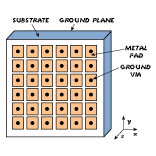
The dominant surface wave in most practical microstrip patch antennas on a grounded dielectric substrate is the TM0 mode, which has no cutoff frequency. Therefore, a 2-D lattice that can prohibit the propagation of the TM0 mode  along the dielectric substrate was sought. Figure 1 shows a schematic of the proposed 2-D PBG structure, which consists of a square lattice of small metal pads with grounding vias in the center. This structure can be regarded as the planar version of a more general three-dimensional metallodielectric PBG crystal reported recently by two of the authors.13 Comprehensive full-wave electromagnetic simulations based on the FDTD method in association with proper absorbing and periodic boundary conditions have been performed to analyze the propagation characteristics of this PBG lattice.
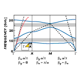
 Figure 2 shows the dispersion diagram of the 2-D PBG lattice, which consists of square pads with 88 mil edge lengths and 8 mil gaps. The grounding via in the center of each pad has a diameter of 8 mil, and the substrate is 25-mil-thick Duroid with er = 10.2. The three sections in the graph refer to different directions of wave propagation. For each section, the propagation vector b in the wave vector space is varied along the edges of the irreducible Brillouin zone (BZ) (shaded triangle in the inset). The dotted straight lines represent the propagation in air and in a homogeneous medium with a dielectric constant of 10.2 (equal to that of the substrate). The dash-dot line to the left of the diagram is relative to the TM0 mode of the grounded dielectric slab without the PBG lattice. This mode has no cutoff frequency and is responsible for surface wave power losses in most practical patch antennas.
Meanwhile, the three continuous lines represent the lowest order modes of the PBG structure. It can be seen that two complete band gaps exist, which forbid propagation in the 8.60 to 12.66 GHz and 23.44 to 27.36 GHz frequency ranges regardless of the polarization and direction of wave propagation. Figure 3 shows the distribution of electric energy density as well as the electric and magnetic vector fields of the first mode at point X (bx = p /a, by = 0, bz = 0) of the BZ. These quantities are shown for a single unit cell of the periodic structure and on the plane z = 0.44 mm located inside the substrate and parallel to the ground plane. At point X of the BZ, this mode has a frequency of 8.48 GHz and a strong longitudinal component of the electric field located mainly in the gaps between metallic pads while the magnetic field circulates around the vias. Due to the presence of the strong longitudinal electric field component, this mode can be classified as a TM mode. The electric energy density and the electric and magnetic vector fields of the second mode at the same point X are also shown. The frequency of this mode for the chosen value of propagation constant is 19.02 GHz. This mode can be classified as TE because it has a strong longitudinal component of magnetic field and electric field mainly transverse to the direction of propagation. Consequently, the TM0 surface wave cannot couple to this mode. In other words, the band
