Figure 1 Idealized transistor I-V curves (a) and I-V curves for NE5550779A FET (b).
A 460 MHz Class J power amplifier achieves a drain efficiency greater than 80 percent at 4 W output power with a 7.5 V supply. Detailed analysis is provided, noting assumptions used and their implications on circuit realization. Performance measurements are in good agreement with the analytical predictions.
Today, short-range wireless communication systems are increasingly employed for various applications. These systems usually operate in sub-GHz frequency bands for better radio wave propagation and include portable wireless devices powered by relatively low battery supply voltages. Consequently, one of the critical development challenges for these wireless systems is the design of a high efficiency power amplifier at the chosen frequency and required supply voltage.
High efficiency power amplifier design has long been an interest of RF engineers and is a topic widely covered in the literature. While classical high efficiency amplifiers, Class AB/B/C, are still discussed in most textbooks on RF amplifier designs,1,2 recent research activities are focused on various switch-mode amplifiers such as Class E and Class F.3,4 Lately, another type of high efficiency power amplifier, Class J, first introduced in 2006,5 has gained the attention of design engineers as well as researchers for the simplicity of its matching networks and relevance in real circuit designs.6,7,8 In this article, a review of the Class J power amplifier is presented along with an outlined design approach using the Class J concept for a 460 MHz power amplifier. The amplifier achieves a drain efficiency of more than 80 percent at 4 W output power with a 7.5 V supply. The device used in the design is Renesas’ Silicon Power LDMOS FET, NE5550779A. It has rated output power of 7 W and is suitable for VHF to UHF applications with relatively low supply voltages (< 10 V).
CLASS J POWER AMPLIFIER BACKGROUND
The Class J amplifier was first proposed by Cripps5 in 2006, followed by a more systematic analysis in 2009.6 Since then there has been a significant number of publications on this mode of operation, mostly found in academic journals or white company papers, where a detailed treatment is usually omitted. Here, the principle of a Class J amplifier is provided in detailed steps, with particular attention paid to the assumptions used in circuit analyses and their implications on circuit realization.
Like classical high-efficiency linear amplifiers such as Class B, Class J is also considered a linear amplifier in that the drain current is assumed to be controlled only by the input level (gate voltage in the case of LDMOS) and is independent of the drain voltage. The difference between them is in the output load condition. For Class B, it is assumed that all harmonics are shorted at the output and therefore only the fundamental and DC components exist in the drain voltage. The actual circuit implementation of such a condition (all harmonics being shorted) is not always realistic, however, even at moderately high frequencies due to the presence of the internal output capacitance, Cout.5 In the Class J mode, the second harmonic reactive component associated with Cout is actually utilized in combination with an appropriate fundamental load impedance to generate the so-called flattening effect on the drain-voltage waveform. This effect allows a further increase in the fundamental amplitude of the drain voltage such that the same efficiency and output power of a Class B amplifier can be achieved.

Figure 2 Equivalent circuit and half-sine waveform of id.
TRANSISTOR MODEL AND EQUIVALENT CIRCUIT
The transistor used in the Class J analysis is characterized, in the same manner as that for classical linear amplifiers, by a set of highly idealized I-V curves as shown in Figure 1a. In this idealization, the drain current, id is assumed to be flat (independent of the drain voltage, vd). Therefore, the transistor can be modeled as a controlled current source. The knee voltage denoted by Vk in Figure 1a marks the transition voltage below which the linear assumption is no longer valid. The requirement that vd ≥ Vk is a crucial condition in the analysis of linear amplifiers. For simplicity, Vk = 0 is assumed and, as a result, the constraint that vd ≥ 0 is used throughout this article. When compared with experimental data, an effective DC voltage, Vdc-Vk should be used in the place of Vdc in the formulas obtained in this article. Furthermore, actual I-V curves change gradually and Vk can only be estimated. Figure 1b shows measured data in the knee voltage area for the NE5550779A transistor.
With the transistor modeled as a current source, the complete equivalent circuit is shown in Figure 2. In principle, the equation for the drain voltage can be solved in the frequency domain when the Fourier components of the drain current, id and the load impedance, Z are known:

Figure 3 Flattening effect of the second harmonic component.

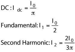
where n is the index for nth harmonic. For the Class J PA, it is assumed that the second harmonic, vd2 is present and all higher harmonic components are shorted, i.e., vdn = 0 for n > 2. Consequently, only the first three Fourier components of id must be considered. In addition, as in the Class B analysis, id is assumed to be a half-sine wave (the conduction angle is π). Then the drain current can be written as:2

here θ= ωt, and the amplitudes are explicitly given by:

where I0 is the amplitude of the half-sine wave (see Figure 2). Correspondingly, the drain voltage has the form:


Figure 4 460 MHz circuit board.
In Equation 3, Vdc is the same as the supply voltage, and vd1 and vd2 can be expressed as:

The negative sign is the result of the convention used for the current source indicated in Figure 2.
VdWAVEFORM AND THE FLATTENING EFFECT
When the drain voltage contains only the DC and fundamental components, the maximum fundamental amplitude is the same as the DC value due to the constraint of vd ≥ 0, as illustrated by the plot of y = 1 + cos(x) in Figure 3. The figure also shows that when a second harmonic component, 0.4cos(2x), is added, the bottom part of the new waveform is flattened. This implies that the addition of a second harmonic component with an appropriate phase allows the fundamental component to further increase without changing the DC level. Evidently the increase in drain voltage at the fundamental frequency can potentially boost the output power, and therefore the efficiency. This flattening effect associated with the second harmonic component is the basic idea behind Class J operation. The task for Class J PA analysis is to determine the appropriate phase and amplitude relationships between the fundamental and second harmonic components such that the fundamental amplitude is maximized while the overall waveform satisfies the constraint that vd ≥ 0.

Figure 5 460 MHz circuit board schematic.

Figure 6 460 MHz evaluation board - typical performance.
Consider a general form for waveforms that have the first three Fourier components:

here all amplitudes are normalized to the DC value. To maximize the voltage swing while still in compliance with the constraint vd ≥ 0, the waveform in Equation 5 should reach 0 at its lowest points. Let θ0 be the location of the lowest point of vd (θ), then we require

Equation 7 is due simply to the fact that a function’s derivative is zero at its minimum point. It turns out that the mathematical solution for θ0 is quite tedious for the general expression in Equation 5. The analysis can be done with a simplified expression as described in the next section.

Figure 7 Setup for output load impedance simulation.
CLASS J MODE OF OPERATION
A special case of Equation 5 that is in factored form is used to analyze the Class J PA:6

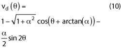
Equation 8 has an obvious solution, θ0 = 0 that simultaneously satisfies Equations 6 and 7. It can be proved that for |α| < 1 , θ0 = 0 is the only solution. For |α| = 1, there is a second solution in addition to θ0 = 0. When |α| > 1, θ0 = 0 is only a local minimum and the requirement of vd ≥ 0 is no longer true in certain regions of θ. Therefore, |α| ≤ 1 is the range of αthat corresponds to physically meaningful solutions.
It will be proven that the waveform described by Equation 8 represents a class of amplifiers that have the same output power and efficiency. The parameter, α in the equation is a distinguishing attribute for this class of amplifiers with a range of |α| ≤ 1. At a= 0, vd is reduced to the classical Class B mode (only DC and fundamental components exist). While Class J is sometimes defined in the literature as a special case for α = 1, in this article “Class J” is used loosely for the entire class of waveforms described by Equation 8. In the following, the load impedances that will generate the required Class J waveforms are derived.
Equation 8 can be rewritten as:

With trigonometric identities, vd (θ) can be further explicitly expressed as a sum of three Fourier components:

Now if the fundamental load impedance, Z1 is chosen to be in the form of:

then, the amplitude and phase of Z1 in the phasor form,

and Θ0 = arctan (α) repectively. Using Equations 2 and 4, the fundamental drain voltage is

The second harmonic load impedance is chosen as a pure reactance:

It is confirmed in the next section that such a form of Z2 is realistic for real circuit designs. This is because the external matching network is usually a type of lowpass filter and the dominant contribution to the second harmonic impedance is the internal output capacitance.
The drain voltage at the second harmonic becomes:

Including the DC term, the complete expression for vd is

When R is chosen to be:

Equation 15 becomes exactly the same as Equation 10. So the impedances defined in Equation 11 and 13 lead to the drain voltage waveform of the Class J mode defined in Equation 8 (note in Equation 8 Vdc is normalized to unity).
The power delivered to the load at the fundamental frequency is

where V1R is the amplitude of the in-phase (with current, id1) component of the fundamental drain voltage and is given by

Here, Equations 12 and 16 are used. Thus

On the other hand, using the expression for Idc in Equation 2 the DC power is obtained as

Therefore, the drain efficiency is


Figure 8 Load impedance simulation of the standard evaluation circuit.
This confirms the output power and drain efficiency for this class of linear power amplifiers are independent of the parameter a.
So far, it has been shown that Class J is a class of linear high efficiency power amplifiers whose drain voltage waveform and load impedance can be uniformly described by Equations 8, 11 and 13. The members of this class of amplifiers are characterized by a parameter, awhich has a valid range of |α| ≤ 1. Mathematically, the classical Class B mode is just a special case of the Class J PA for α = 0. However it can be proved (the details are not presented here) that when α approaches 0, the circuit realization for the required load impedance described in Equations 11 and 13 becomes unrealistic. So, to achieve true Class B mode operation in practice, a classical approach of a parallel resonant circuit is still required. In the next section, a circuit realization of the Class J PA with α ~ 0.5 is presented.
CIRCUIT REALIZATION FOR MAXIMUM OUTPUT POWER
The device used for this design is Renesas’ medium power LDMOS transistor, NE5550779A. It performs well with relatively low supply voltages ranging from 3.5 to 9 V, and therefore is suitable for battery operation. It has up to a 7 W output power capability, which is in a typical range for portable wireless devices. The chosen operating frequency is 460 MHz, a popular band for short range wireless communications.
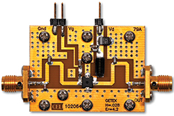
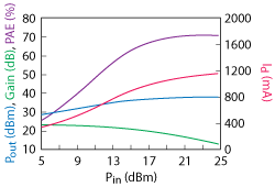
Several standard evaluation circuit boards for the NE5550779A, tuned for different frequency bands, are available from California Eastern Laboratories. Figure 4 is a photo of the circuit board and Figure 5 shows the 460 MHz circuit schematic. The matching networks consist of multiple sections of shunt capacitors and serial transmission lines, a circuit topology commonly used in practice. The lowpass nature of the network is what is required by the Class J analysis. The input matching network is designed for good return loss while the output matching is tuned for maximum saturated output power. Typical performance plots with a 7.5 V supply are shown in Figure 6. As the data indicates, 38 dBm of output power and greater than 70 percent PAE are achieved with an input power of 20 dBm.
The impedance of the output matching network seen from the transistor’s internal current source is analyzed using Keysight’s design software, ADS. The simulation setup is shown in Figure 7. In addition to the external matching components, a shunt capacitor (C4) and serial inductor (L1) are included in the matching network to account for the effects of transistor internal output capacitance and package inductance. Figure 8 shows the calculated impedance in a Smith chart format. As the marker, m1, in the plot indicates, the fundamental-frequency impedance is essentially purely resistive at about 5.7 Ω. For a linear power amplifier, the relationship between the output power, Pout, and optimal load resistance Ropt is described by a classical formula:3


Figure 9 Load impedance simulation after tuning for the Class J mode.
When using Equation 22 for estimating actual circuit performance, the knee voltage Vk should be subtracted from the supply voltage for Vdc. In this case, if Vk is taken as 1 V (see the actual I-V curve in Figure 1b) then Pout = 3.7 W (35.6 dBm) for Ropt = 5.7 Ω. In reference to the plots in Figure 6, this output power level indeed corresponds to an input power level (around 13 dBm) where the amplifier starts to significantly deviate from the linear region. Beyond the linear region, the plot shows that efficiency further increases along with input power, which is a well known fact. From an analytical perspective, in the nonlinear region the drain current is no longer independent of the drain voltage and the simple current source model breaks down. The exact circuit behavior in the region vd < Vk depends on the details of the id vs. vd characteristics and the load-termination condition. Some quantitative results that are based on much simplified circuit models have been reported on circuit performance in this region.2,9 While accurate predictions of the circuit behavior in the nonlinear region can perhaps be determined from a simulation with an appropriate nonlinear device model, analytical works based on simple models do demonstrate that the output power and efficiency can be further increased along with the input power in this region.
CIRCUIT USING CLASS J CONCEPT
It was found that by tuning the circuit components with the ADS tuning tool (see Figure 7) the relationship between the fundamental and second harmonic load impedances described in Equations 11 and 13 can be achieved, as illustrated in Figure 9. Specifically, after changing C3 from 15 to 20 pF and TL2 from 13° to 14.64°, the load impedance becomes:

This confirms that Z2 is indeed nearly purely reactive. It can also be seen that the numerical values of Z1 and Z2 are within 5 percent of the values for the Class J mode if R = 10.1 Ω and α = 0.52 are used in Equations 11 and 13. This observation suggests that Class J mode operation can be realized on the existing circuit board with some simple changes to component values.
Figure 10 shows the performance of the actual circuit with the Class J matching network of Figure 9 implemented. A distinctive difference in Figure 10 versus Figure 6, is that efficiency at an input power level of around 13 dBm, the region where linear-to-nonlinear transition occurs, is significantly higher (PAE changes from 55 to 72 percent), while the output power is similar to that in Figure 6. This confirms that the Class J concept can be utilized in real circuit designs to achieve high efficiency, particularly in the linear region. Beyond the linear region the efficiency continues to increase with input power while the output power increases at a much lower rate. Eventually the drain efficiency exceeds 80 percent and the PAE peaks at 78 percent.

Figure 10 Actual performance with the Class J matching network.
The output power saturates at a level of around 4 W, considerably lower than what was achieved on the standard circuit. The reduced saturation level for output power is due to a modified output load line condition that imposes a more severe restriction on the drain current in the nonlinear region, vd < Vk. The effect of load-line matching on output power is discussed in many textbooks.3 In practical design, this trade-off between efficiency and saturated output power is a consideration designers should keep in mind when seeking high efficiency performance.
Another noticeable feature of the plot in Figure 10 is that efficiency remains high (PAE > 70 percent) over a wide range (more than a decade) of input power. This feature makes high efficiency performance relatively insensitive to the input power, which is desirable in certain situations.
Finally, in many applications the saturation point of the PA output power is required to be limited at a certain level. It is found that the same tuning process (i.e., changing C3 and TL1/2 in Figure 7) used for Class J operation can be carried out on the bench to adjust the saturated power level while maintaining high efficiency (see Table 1). The data points in the table are taken at an output power level roughly 0.25 dB below full saturation. As the data shows, the output power saturation point can be adjusted from roughly 1 to 5 W, a power range commonly used in short range communication systems, while PAE remains at a relatively high level (greater than 74 percent). This technique allows designers to use the same device to achieve high efficiency at different saturated output power levels. In principle, some power capability is wasted when a power transistor is used at power levels significantly lower than its capability. Nevertheless, using one device for multiple designs with different output power specifications may be advantageous, considering that for the power and frequency ranges discussed in this article the pricing difference among different devices is often manageable.
CONCLUSION
Utilizing the flattening effect associated with the second harmonic component in the drain voltage waveform to increase the fundamental amplitude, and thus to increase efficiency, is the key concept of the Class J power amplifier. In this article, a PA design employing Renesas’ NE5550779A using the Class J concept is demonstrated for 460 MHz applications. It is shown that the load impedances required for Class J operation can be realized with a commonly used circuit topology. A relatively simple simulation with an EAD tool on the load network can facilitate the process to determine appropriate component values. Sophisticated nonlinear models are helpful but not necessary. In fact, the same results can be achieved with bench tuning without performing any simulations. Performance measurements on an actual circuit with a Class J load network are in good agreement with the analytical predictions. The circuit yields a drain efficiency of 80 percent with a PAE of 78 percent. The boosted efficiency, along with a much wider range of allowable input power to yield high efficiency, makes the Class J PA a suitable circuit choice in many real-world applications.
References
- F. Sechi and M. Bujatti, “Solid-State Microwave High-Power Amplifiers,” Artech House, Norwood, Mass., 2009.
- M. Albulet, “RF Power Amplifiers,” Noble Publishing, 2001.
- P. Colantonio, F. Giannini and E. Limiti, “High Efficiency RF and Microwave Solid State Power Amplifiers,” John Wiley & Sons Ltd., 2009.
- A. Grebennikov, N.O. Sokal and M.J. Franco, “Switchmode RF and Microwave Power Amplifiers,” 2nd Edition, Academic Press, 2012.
- S. C. Cripps, “RF Power Amplifiers for Wireless Communications,” 2nd Edition, Artech House, Norwood, Mass, 2006.
- S. C. Cripps, P. J. Tasker, A. L. Clarke, J. Lees and J. Benedikt, “On the Continuity of High Efficiency Modes in Linear RF Power Amplifiers,” IEEE Microwave and Wireless Components Letters, Vol. 19, No. 10, October 2009, pp. 665]667.
- S. Rezaei, L. Belostotski, F. Ghannouchi and P. Aflaki, “Integrated Design of a Class J Power Amplifier,” IEEE Transactions on Microwave Theory and Techniques, Vol. 61, No. 4, April 2013, pp. 1639]1648.
- J. Moon, J. Kim and B. Kim, “Investigation of a Class J Power Amplifier with a Nonlinear Cout for Optimized Operation,” IEEE Transactions on Microwave Theory and Techniques, Vol. 58, No. 11, November 2010, pp. 2800]2811.
- M. Dong, “Design Study of a High Efficiency LDMOS RF Amplifier,” High Frequency Electronics, July 2011, pp. 36]50.
Mouqun Dong is an RF engineer with California Eastern Laboratories. He received his Ph.D. degree in physics from Syracuse University in 1996, and M.Sc. and B.S. degrees in physics, from Chinese Academy of Sciences and Beijing Jiaotong University respectively.
