60 and 120 W, 2 GHz LDMOS FETs
Ericsson Components, RF Power Products
Morgan Hill, CA
The dramatic increase in cellular traffic has necessitated the use of spread spectrum techniques such as time-division multiple access (TDMA) and code-division multiple access (CDMA). These modulation methods have significantly tightened the linearity requirements for today’s base station amplifiers.
Two new laterally diffused metal-oxide semiconductor (LDMOS) FETs have been developed specifically for CDMA and TDMA applications from 1.8 to 2 GHz. The types PTE 10112 and PTE 10120 LDMOS FETs are rated at 60 and 120 W (min) output power, respectively. Both FETs feature ion implantation, nitride surface passivation and gold metallization to ensure a long lifetime and good reliability. In addition, both types offer 100 percent lot traceability.
LDMOS Advantages
 A cross-sectional view of an LDMOS FET is shown in Figure 1 . The FET operates in the enhancement mode; that is, with a positive-polarity drain voltage applied, no drain current flows until a positive gate voltage enhances a channel across the p well. During operation, the channel current is modulated by the signal impressed on the gate.
The source is brought to the bottom side of the die to lower the source inductance and improve the intrinsic gain. The die also can be attached directly to the flange of a package, reducing thermal resistance. By virtue of the isolated gate electrode, the resulting DC input impedance is high, allowing for a simple resistive bias network. This simple bias scheme reduces circuit complexity and cost compared to the active bias network required for a bipolar junction transistor (BJT).
Another MOSFET advantage is thermal stability. The FET’s drain current decreases with increasing temperature. The threshold voltage also is temperature dependent, but under large drain currents the combined effect produces a drain current that is proportional to temperature, which results in complete absence of thermal runaway.
The LDMOS process has improved RF performance significantly by lowering the drain-to-gate capacitance. This lower capacitance not only improves the device’s gain, but also produces better device stability. In addition, because the source is located on the bottom of the die, source inductance due to the bond wires is eliminated. These source wires are required on vertical MOSFET structures. This source inductance acts as degenerative feedback, thus lowering gain. The LDMOS transistor offers a 3 dB gain improvement compared to a BJT with similar power capability.
A comparison of two-tone third-order intermodulation (IM) distortion between the FET and BJT indicates that the BJT has optimum IM performance near its rated power that becomes worse as the output is varied above and below this level. On the other hand, the FET exhibits worse IM at the upper end of its power rating but surpasses the BJT as the power is backed off from maximum. The LDMOS transistor’s IM distortion has a monotonic slope with output power.
In general, the LDMOS transistor offers improved gain performance, better thermal stability and improved IM distortion when the power is backed off as compared to a BJT. When biased at an optimum quiescent current, the gain of the FET can be held constant over a wide range of input power, allowing the use of a class AB stage where a class A stage was required previously.
Device Performance
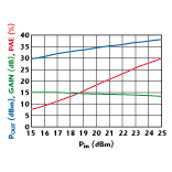
As a result of these LDMOS advantages, the two new power FETs feature higher gain, increased efficiency, 42 percent higher power and low IDQ drift, providing maximum RF signal power at a lower cost. The PTE 10112 transistor provides 60 W (min) power output at the 1 dB compression point (P1dB) with a typical gain of 12 dB. Figure 2 shows the device’s output power vs. input power at 2 GHz with a VCC of 28 V and IDQ of 580 mA. Drain efficiency is 41 percent and the device is inherently stable at a maximum SWR of 10 rotated through all phases.
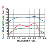
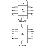
 Figure 3 shows the PTE 10112 device’s typical output power, gain and efficiency at P1dB vs. frequency at VCC = 28 V and IDQ = 580 mA. Maximum ratings for the PTE 10112 include VDSS of 65 V DC, VGS of ±20 V DC, an operating junction temperature TJ of 200°C, total device dissipation at 25°C flange temperature of 237 W and a thermal resistance of 0.74°C/W. The PTE 10112 device is supplied in a type 20248 gold-metallized flange-mount package.
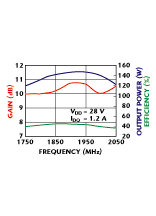
The PTE 10120 LDMOS FET is a higher power push-pull version, supplying 120 W (min) power output at P1dB at VDD = 28 V and IDQ = 1.2 A at 2 GHz. Its typical gain is 11 dB and drain efficiency at 120 W output is 40 percent. Total device dissipation is 440 W and thermal resistance is 0.39°C/W. Other maximum ratings are similar to the PTE 10112 device. Figures 4 and 5 show the PTE 10120 FET’s typical output power vs. input power, and output power, gain and efficiency at P1dB vs. frequency, respectively. The PTE 10120 device is housed in a type 20250 gold-metallized flange-mount package.


Conclusion
The PTE 10112 and PTE 10120 LDMOS FETs are common-source, n-channel, enhancement-mode transistors rated at 60 and 120 W minimum output power, respectively, that are intended specifically for CDMA and TDMA cellular base station applications at 1.8 to 2 GHz. The devices feature ion implantation, nitride surface passivation and gold metallization to ensure superior performance as well as good device lifetime and reliability.
Ericsson Components, RF Power Products,
Morgan Hill, CA
(877) 465-3667.
