
A novel defected microstrip structure (DMS), which behaves in a way similar to the known defected ground structure (DGS) unit cell,1–10 is studied in this article. The unit DMS3,4 is made by etching slots in the microstrip line, which then exhibits the property of rejecting microwaves at certain frequencies. Due to its simple planar structure and ease of fabrication by a photolithographic process, DGS is widely used in microwave passive circuits, such as filters,2,5,6 antennas4,7,8 and oscillators.9,10 Because of the leakage through the ground plane, the problems of enclosure should be considered when DGS is used to design microwave circuits. In the DMS case, the defected cell is etched in the center conductor and there is no leakage through the ground plane. This structure can be integrated more easily with other microwave circuits and the filter and antenna dimensions can be effectively reduced by using DMS.4
Based on EM simulation results, a circuit model of the DMS is established and the lumped elements of this model are extracted according to circuit theory. The stop-band effect of the presented DMS can be explained by employing the extracted parameters and circuit theory. In order to show the effectiveness of the proposed scheme, two types of three-pole low pass filters and a five-pole low pass filter (LPF) are designed using DMS to improve their stop-band characteristics. The results measured on the five-pole LPF agree well with the simulation.

Frequency Characteristics of the Defected Microstrip Structure
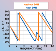
The novel defected microstrip structure (DMS), which consists of a rectangular slot of length l and width b etched in the middle of the center conductor and a small slot of width g perpendicular and in the center of the main slot, is shown in Figure 1. The width of the microstrip line is then W = b + 2c. Similarly to DGS, the DMS increases the electric length of microstrip and disturbs the current distribution. The effective capacitance and inductance of the microstrip line increase. Accordingly, a microstrip with a unit DMS has a stop-band and slow-wave characteristics. Novel compact microwave components can be designed by using these characteristics. It can be seen from Figures 2 and 3 that for a 50 Ω microstrip line with l = 13 mm, b = 1 mm, c = 0.8 mm and g = 0.2 mm, the cut-off frequency fc and the attenuation pole frequency f0 are 3.57 and 7.25 GHz, respectively.
In order to probe the relationships between the etched slot dimensions and the characteristics of the stop-band, a 50 Ω microstrip, with a substrate relative dielectric constant of εr = 2.2 and h = 0.762 mm, is chosen for all simulations. Considering the limited width of the center conductor, the parameters b = 1 and c = 0.8 mm are fixed in the following calculations. Thus, the proposed DMS can be fully described by the length l and the slot width g.
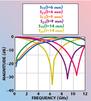
The influence of the length l on the frequency characteristics is simulated with an electromagnetic (EM) simulator while the gap g is kept constant and equal to 0.2 mm. Figure 4 shows the simulation results for three different lengths l. The stop-band frequency decreases when the length l increases. The reason is that the large slot area is directly related to the effective inductance. As the length l is increased, the effective inductance increases, and the increasing inductance gives rise to a lower stop-band. At the same time, the width g of the etched gap also influences the stop-band frequency.2 To investigate the influence of the gap g, the length l is kept constant and equal to 13 mm. Figure 5 shows the simulated results for three different gaps. It can be seen that as the width of the etched gap increases, the location of the attenuation pole increases. The reason is that the gap affects the effective capacitance. The increased gap width leads to a lower capacitance and the lower capacitance results in a higher resonance frequency f0. Different stop-bands can be obtained by adjusting the length l and gap width g of the DMS and the length l affects the location of stop-band more effectively. The DGS has similar stop-band characteristics to the unit cell DMS, so the equivalent circuit model of DGS2 can be used to extract the equivalent circuit parameters of DMS.
Modeling and Parameter Extraction of DMS
The electrical characteristics of the DMS stop-band are simulated as a parallel LC resonance circuit,2,5,6 as shown in Figure 6. The equivalent parameters of the parallel LC circuit of the DMS can be extracted from the EM simulation results. The equivalent circuit of the DMS is matched to the one-pole Butterworth LPF response. The reactance of the DMS can be expressed as

where
ω0 = resonance angular frequency of the parallel LC resonator
The series inductance of the one-pole Butterworth LPF can be written as
![]()
where
ω' = normalized angular frequency
Z0 = characteristic impedance
g1 = normalized parameter of
one-pole Butterworth LPF

According to circuit theory, the two reactance values must be equal at wc, that is
![]()
where
ωc = cut-off angular frequency of the parallel LC resonator
From Equations 1, 2 and 3, the inductance L and the capacitance C can be obtained as


where ƒ0 is the resonant frequency, which can be obtained from the EM simulation results. The equivalent-circuit parameters can be calculated from Equations 4 and 5. The values of the lumped-element parameters for the proposed DMS are shown in Table 1.

The simulated frequency response of the extracted equivalent circuit parameters for a 50 Ω microstrip with unit DMS have been shown previously and compared with the EM simulation. It shows an excellent agreement between the EM simulation and the calculated circuit simulation. The calculated equivalent circuit parameters of the unit DMS are C = 0.1428 pF and L = 3.3766 nH. A small discrepancy still exists between the two simulations because the LC parallel circuit is an ideal model and the loss of the resistor and radiation are not considered.
Design of A Three-pole LPF and Five-pole LPF Using DMS
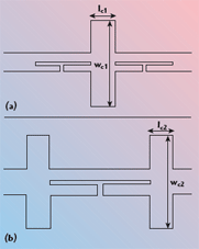
In order to verify the stop-band validity of the DMS, two types of three-pole low pass filters are designed and shown in Figure 7. The dimensions of the DMS are the same as before. According to transmission line theory, if an open stub, with a characteristic impedance Z0, is shorter than λg/4, it can be used to realize a shunt capacitance.11,12 In an LPF with two DMSs, the shunt capacitor can be realized by using a crossed open stub. The width of the stub is wc1 and its length is lc1. Two series inductances are realized by using two DMSs, on both sides of the stub. In another LPF with unit DMS, two identical stubs with a width ωc2 and length lc2 are used as series inductances on both sides of a unit DMS. The optimized dimensions of the stubs that are calculated with the EM simulator are lc1 = 3.3 mm, ωc1 = 14.54 mm, lc2 = 2.9 mm, ωc2 = 16.2 mm. The simulated S-parameters of the two low pass filters are shown in Figure 8. It can be seen that in the low pass-band, the maximum ripple level is –0.08 dB; the S21 parameters are less than –15 dB. In the whole stop-band, the maximum insertion losses of both filters are better than –20 dB. The excellent band-gap performance of DMS is demonstrated.

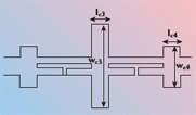
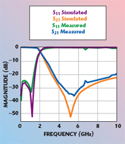
In order to improve the insertion loss performance of the LPF, a five-pole LPF is designed using two DMSs, as shown in Figure 9. This filter is realized by setting two higher impedance identical open stubs on each sides of the three-pole LPF with two DMSs. The optimized dimensions of two different stubs can be obtained with the help of an EM simulator. They are lc3 = lc4 = 2.9 mm, ωc3 = 18.7 mm, ωc4 = 7.9 mm. The EM simulated and measured results of a five-pole low pass filter are shown in Figure 10. The measurements are taken with a HP8510 vector network analyzer. There is only a slight difference between the two results. It can be seen from the measured results that there is an attenuation pole at 5.5 GHz, and the insertion loss characteristics are improved in the whole stop-band while the return losses are more than 25 dB in the low pass-band.
Conclusion
In this article, a novel defected microstrip structure (DMS) and its equivalent circuit are studied. In comparison with a defected grounded structure (DGS), there is no increment of leakage from the ground plane by using DMS. There is also no enclosure problem for this novel defect structure, because it is etched on the center conductor. In order to show the validity of DMS and its characteristics, three types of low pass filters are designed with DMS. Due to the DMS resonance, the three LPFs have wider and deeper stop-band performances than that of conventional LPFs. Finally, the response of a five-pole LPF has been measured, which shows an excellent insertion loss characteristic.
Acknowledgment
This work is supported by the Foundation of Antenna and Microwave Key Laboratory in China (No. 51437080204QT0601) and the National Natural Science Foundation of China (No. 60571054).
References
1. C.S. Kim, J.S. Park, D. Ahn and J.B. Lim, “A Novel 1D Periodic Defected Ground Structure for Planar Circuits,” IEEE Microwave and Guided Wave Letters, Vol. 10, No. 4, 2000, pp.131–33.
2. D. Ahn, J.S. Park, C.S. Kim, Y. Qian and T. Itoh, “A Design of the Low Pass Filter Using the Novel Microstrip Defected Ground Structure,” IEEE Transactions on Microwave Theory and Techniques, Vol. 49, No. 1, January 2001, pp. 86–93.

3. J.A. Tirado-Mendez and H. Jardon-Aguilar, “Comparison of Defected Ground Structure (DGS) and Defected Microstrip Structure (DMS) Behavior at High Frequencies,” First International Conference on Electrical and Electronics Engineering (ICEEE) Digest, 2004, pp. 7–10.
4. J.A. Tirado-Mendez, H. Jardon-Aguilar, F. Iturbide-Sanchez, I. Garcia-Ruiz, V. Molina-Lopez and R. Acevo-Herrera, “A Proposed Defected Microstrip Structure (DMS) Behavior for Reducing Rectangular Patch Antenna Size,” Microwave and Optical Technology Letters, Vol. 43, No. 6, 2004, pp. 481–484.
5. J.S. Lim, C.H. Kim, D. Ahn, Y.C. Jeong and S. Nam, “Design of Low Pass Filters Using Defected Grounded Structure,” IEEE Transactions on Microwave Theory and Techniques, Vol. 53, No. 8, August 2005, pp. 2539–2554.
6. X.H. Guan, G.H. Li and Z.W. Ma, “A Novel Low Pass Filter Using Defected Ground Structure,” Microwave and Optical Technology Letters, Vol. 46, No. 1, 2005, pp. 17–20.
7. Y.J. Sung, M. Kim and Y.S. Kim, “Harmonics Reduction with Defected Ground Structure for a Microstrip Patch Antenna,” IEEE Antennas and Wireless Propagation Letters, Vol. 2, No. 1, January 2003, pp. 111–113.
8. Y. Chung, S.S. Jeon, A. Dal, J.I. Choi and T. Itoh, “High Isolation Dual-polarized Patch Antenna Using Integrated Defected Ground Structure, IEEE Microwave and Wireless Components Letters, Vol. 14, No. 1, January 2004, pp. 4–6.
9. J.S. Park and M.S. Jung, “A Novel Defected Ground Structure for an Active Device Mounting and its Application to a Microwave Oscillator, IEEE Microwave and Wireless Components Letters, Vol. 14, No. 5, May 2004, pp. 198–200.
10. M.S. Joung, J.S. Park and H.S. Kim, “A Novel Modeling Method for Defected Ground Structure Using Adaptive Frequency Sampling and its Application to Microwave Oscillator Design,” IEEE Transactions on Magnetics, Vol. 41, No . 5, May 2005, pp. 1656–1659.
11. J.S. Hong and M.J. Lancaster, Microstrip Filters for RF and Microwave Applications, John Wiley & Sons Inc., New York, NY, 2000, pp. 89–102.
12. G. Matthaei, L. Young and E.M.T. Jones, Microwave Filters, Impedance-matching Network and Coupling Structures, McGraw-Hill, New York, NY, 1964, pp. 360–364.
Sheng Zhang received his BS degree from Anhui Normal University, China, in 2000, and his MS degree from the Hefei University of Technology, China, in 2004. He is currently working toward his PhD degree at Shanghai University, China. His research interests include electromagnetic band gaps, substrate integrated waveguides and passive microwave components.
Jian-Kang Xiao received his BS degree in electronics in 1996 and his MS degree in radio physics from Lanzhou University in 2004. Since then, he has been an electrical engineer at the Institute of Modern Physics, Chinese Academy of Sciences. He is currently working toward his PhD degree at Shanghai University, China. His research interests include microwave and millimeter-wave theory and technologies.
Zi-Hua Wang received his BS degree from the Harbin Institute of Technology, China, in 1968, and his MS degree from the Shanghai University of Science and Technology, China, in 1981. He is now a professor at the school of Communication and Information Engineering, Shanghai University. His research interests include fiber and integrated optics, microwave theory and technology, and antennas.
Ying Li is currently a professor at Shanghai University. His research interests include electromagnetic theory, microwave and millimeter-wave techniques and their applications.
