
Current trends in modern wireless communications systems require advanced digital signals to handle high data throughput. The wider frequency bandwidth of a data-containing signal channel, along with sophisticated digital modulation, result in stringent signal-to-noise ratio (SNR) requirements to maintain affordable data loss (bit error rate (BER), packet/frame error rate (PER/ FER), etc.). For instance, digital video broadcasting (DVB) and wireless local area network (WLAN) systems utilize orthogonal frequency division multiplexing (OFDM) wideband signals with multiple sub-carriers, each of which is modulated at a rate much less than the original data-containing signal.1,2 Although inter-symbol interference due to multi-pass propagation is neglected at a certain level, the communication link is limited by distance, depending on the transmitter output power and the receiver sensitivity. Government authorities are closely monitoring transmitter power emission levels and all existing wireless communication standards require upper power limits. As a result, receiver sensitivity enhancement and antenna gain (directivity) remain the only choices to extend communication link distance for a particular standard.
There are many noise sources defining receiver sensitivity.3 The most important are the RF front-end loss between the antenna and the signal demodulator and the noise figure (NF) of the low noise amplifier (LNA). However, there is another, not so obvious noise source in an antenna to demodulator chain — the coupled line loss, which is important when a high signal-to-noise ratio (SNR) is required. This type of loss, as an additional noise source in a receiver chain, is investigated in this article, based on WLAN and DVB-Handheld (DVB-H) systems examples.

Short Coupled Lines in the RF Front-end
Portable devices are getting smaller and the components positions and their interconnecting lines need to be designed correctly to avoid unexpected system performance degradation. Consider two microstrip lines, somewhere in the RF front-end circuit, coupled over a short 1 mm length (see Figure 1). A laminate substrate (such as FR4, GETEK, BT) is chosen with a typical thickness of 0.25 mm with microstrip line widths of 0.2 mm and a pitch of 0.3 mm. These dimensions are typical for WLAN Mini-PCI cards, CardBus32, etc. The positioning of the traces is not as dense as for the already “standard” multi-chip/multi-die modules. Suppose that the useful RF signal is passing through from port 1 to port 2. The line associated with ports 3 and 4 does not necessarily contain an RF signal; it can be some biasing or another line used in the whole circuit. When ports 3 and 4 are simply loaded with 50 Ω (which is pertinent to RF lines), this short coupling area does not usually create problems in an RF system since the coupled power is 50 to 60 dB lower than in the first line at frequencies up to several gigahertz. Just positioning transmit and receive chains not too close to each other is enough for “normal” system operation.

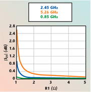
However, if the coupled line is directly connected to ground, capacitors, inductors or resistors, it may create resonances in the line and the coupling with the RF line can be dramatically changed. Such a resonant circuit can be modeled at 2.4 and 5 GHz (WLAN) as well as DVB-H high end frequencies by grounding port 4 through a 1 mm length line and connecting port 3 to an appropriate grounded capacitor. The well-known resonance “killer” is the resistor R1 shown in the circuit. Figure 2 shows the simulated insertion loss in the RF line (between ports 1 and 2), with L2 = 1 mm, C1 = 1.05 pF at 5.26 GHz, C1 = 5.05 pF at 2.45 GHz and C1 = 42.0 pF at 0.85 GHz. The Microwave Office circuit simulator4 was used for the calculations. For simplicity, the capacitance is chosen to be frequency independent and loss less. One can see a large increase in the insertion loss of the RF line, if the resistive loss in the coupled line is small, especially at elevated frequencies. The usual resistive loss of a surface-mount technology (SMT) capacitor is 0.2 to 0.5 Ω at the frequencies considered and one can expect 0.2 to 0.3 dB insertion loss for the 2.4 GHz WLAN receiver, and up to 1 dB for the 5 GHz one. It can be neglected for DVB-H applications. The use of high Q capacitors, associated with coupled lines in RF front-end circuitry, is not suggested in this case. Such behavior is not easily observed if one is monitoring just narrow-band S-parameters and other component characteristics are not tested (or known) separately. The best approach is to avoid resonances near the operating frequencies by an appropriate choice of the trace length and capacitor value. An additional resistor (series or parallel) can be inserted if necessary. This phenomenon has to be understood correctly and differs from the well-known method of noise reduction in digital circuits by introducing a small resistor into a long digital control line.

The phenomenon of an increased insertion loss in an RF line coupled with another resonating line is not only one of the consequences limiting receiver sensitivity. An RF signal created in a resonating line is coupled back to the “original” RF line. This signal is phase-shifted with respect to the “original” RF signal and appears as noise in the main line. Consider the simplified situation when the RF signal PIN is passing through port 1 to port 2. Suppose this signal is coupled from port 1 to port 3 with a coupling coefficient L1, creating a power P2 = PIN/L1 in the coupled line. This attenuated signal is then resonating and coming back to the first line through port 4 to port 2 with a coupling coefficient L2 and a phase change. The returned power is equal to P2 = PIN/(L1L2). If the coupling area is small and homogeneous, L1 = L2 = L. The total power at port 2 consisting of the useful signal and noise is given by
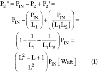

Then the SNR can be defined as (all other noise sources being neglected)
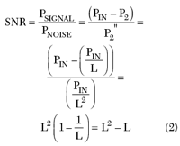
Equation 2 represents the effect of a coupling coefficient between the receiver RF chain line and some neighboring circuit line, the proximity of which can dramatically degrade the sensitivity of a receiver in addition to the “pure” insertion loss increase under the resonating line condition considered above.
Consider as an example the 802.11a WLAN standard requirements regarding the receiver sensitivity. Figure 3 shows a standard noise floor of a receiver for 10 percent PER and the allowed coupling noise, calculated according to Equation 2 for a particular noise figure of the receiver and not taking into account the insertion loss in the coupled lines. It means that, with this coupling noise, the receiver reaches a 10 percent PER with a 3 dB implementation margin for SNR. The figure also shows the receiver noise characteristics for DVB-H mobile (Raleigh fading is taken into account) for multi-protocol frame FER (MFER = 5 percent) and no implementation margin in this case. Figure 4 shows the allowed coupling coefficient between two short lines to pass a standard specification (again without insertion loss consideration). It has to be noted that, although today’s implementation of DVB-H is limited to just 13 Mbps data rate compared to 54 Mbps for WLAN, both system’s receiver noise requirements are severe. Moreover, a 5 dB “typical” receiver noise figure for DVB-H, as stated in the standard, is more difficult to achieve than for the WLAN one (even a 9 dB noise figure could easily pass this specification). The last two figures also show some test data that will be explained later. One can see that a coupling coefficient of approximately 13 dB between the RF receiver line and another line is already detrimental for the high data rate signals of 802.11a systems. The same coupling coefficient has even a severe impact on the noise coupling in DVB-H receivers at high and mid data rates. It has to be noted that DVB-H receivers require a much lower noise figure. Consequently, this coupling has to be taken care of as well during system noise considerations.
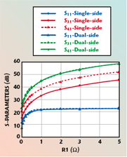
The coupling parameters of the circuit shown previously, with the same circuit element values used to calculate the insertion loss, are shown in Figure 5. One can see that the coupling coefficient is reaching 15 dB in the 5 GHz band for a low series resistance value in the coupled line that, in conjunction with the line insertion loss, can create problems for the receiver sensitivity. The 2.4 GHz band is more resistant to the coupled lines’ noise. The DVB-H high frequency couplings have similar levels as the 2.4 GHz ones and the coupling noise can become bothersome only for the 20 Mbps data rate of future applications.
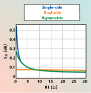
When the resonance in a coupled line is created by two capacitors at the “left” and “right” sides of the 1 mm length coupled area (L2 is disconnected), the insertion loss is slightly higher than for the previous case for reasonable capacitor resistive loss values (0.2 to 0.5 Ω), although it is almost twice as high for very high Q components. Figure 6 shows a comparison of the insertion loss at 5.25 GHz for the cases of a single capacitor, C1 = 1.05 pF, and dual-side capacitors, C1 = C2 = 4.42 pF with L2 and L3 disconnected. At the same time, the coupled noise is considerably lower (see coupling coefficients S31 and S41 in Figure 7).
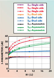
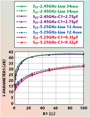
If the resonance is based on distributed transmission lines (microstrip in this case), one can see a considerably lower level of insertion loss in the “main” RF line, compared to the lumped-element resonance of the previous cases (see Figure 8). The greatest influence on insertion loss is noticeable when the coupling area is placed close to the grounded edge of a microstrip line, where the current density is the largest (coupling through magnetic field). Throughout all versions of a coupling area positioning, the coupling coefficients S31 and S41 are well below –25 dB and the noise level increase in the “main” RF line due to the signal coupled back from the resonating line is very small (see Figure 9).
Packaged Devices in RF Receiver Circuits
The placement of components and transmission lines on a PCB is flexible and a PCB board designer can choose the correct layout needed. However, there is not too much freedom in packaged device choices. The package leads can create problems similar to those considered in the previous paragraphs. Consider the plastic LQFP lead-frame package often used in mobile RF circuits (transceivers, front-ends, etc.). A schematic of this package, used in the following simulations, is shown in Figure 10. The balanced receiver LNA inputs have been chosen and one chain of a differential signal is coupled with a neighboring line, resonating at the operating frequencies (upper line in figure). Those lines are coupled through the chip package leads as well as through some short coupled lines placed on the PCB. Four microstrip coupled line sections in the middle, along with inductors, represent the RFIC package leads with bonding wires to the receiver chip. The balanced signal chains passing through the package leads are “screened” by the center lead grounded at the PCB side and as well at a package side. For simplicity, the upper-coupled line, inside the chip, is modeled as a grounded 10 pF capacitor (a reasonable approximation of the biasing decoupling circuit). The external part of this line is modeled either as a microstrip line of an appropriate length (to create a resonance at the frequencies considered) or as a grounded capacitor. The series resistance represents the loss in this line. 3 dB power dividers/combiners, along with 180° phase shifters have been chosen to convert the single-ended signal to a balanced one and vice versa.

Figures 11 and 12 present the simulated insertion loss and coupling coefficients for the LQPF lead- frame package circuit. One can observe a high insertion loss, even in the 2.4 GHz WLAN frequency band, if the biasing coupled line parameters create resonance and the resistive loss in this line is small. It is obvious that a lumped-element resonance elevates the noise level more than a transmission line-based one. One can suggest inserting an artificial loss (series resistor) into this line to increase the sensitivity of a receiver. It has to be noted that the 5 GHz operation is not as good for this package due to fairly long lead traces, even with an appropriate series resistor. The “residual” insertion loss for a receiver is 0.65 to 0.7 dB. At the same time, a series resistor is mandatory in this line to avoid an additional “coupling back” noise from the biasing line to the receiver RF line (see Figures 12 and 4); even a small parasitic external capacitance with a value of 0.3 pF will create a resonance.

A low profile, leadless, QFN plastic molded package is preferred at high frequencies. Figure 13 shows the dramatically decreased insertion loss simulated for the QFN package circuit (similar to the one for the LQFP package and for simplicity TL1 = TL2 = 0). However, the “coupling back” noise is still pertinent to this package and the insertion of at least a small series resistor into the biasing line is suggested (see Figure 14) when the resonance in the neighboring line is close to the operating frequencies.
The simulations show that the LQFP package is not suitable for DVB-H applications due to increased insertion loss with coupled lines. The QFN package has no problems in DVB-H applications. At the same time, the “coupling back” noise is not a problem for both packages with reasonable component losses of 0.2 to 0.5 Ω. The differential signals considered create less coupling than single-ended signals (by approximately 3 dB). Thus, with single-ended RF lines, the coupling has to be verified more carefully. Certainly, the simulations shown have some estimated character due to the circuit simulator used. A 3D simulator used for electro-magnetic structures, however, shows good agreement within 1 dB. Notice that the coupling coefficients are somewhat dependent on the coupled line active resistors modeled in ports 3 and 4.
Test Results
An LQFP-48 lead-frame plastic package with an 802.11a WLAN transceiver placed on a Mini-PCI card has been tested. The equivalent circuit of the receiver section is similar to the one simulated. One of balanced input lines of the receiver is placed near to a control line, modeled as a capacitance of 10 pF at the semiconductor die side and as a 29 mm-long microstrip line and 1 kΩ resistors at ports 3 and 4. The simulation results for this circuit are presented in Figure 15, without a series resistor in the control line. One can see that the long length of the control line creates multiple resonances, one of which is falling into the 5 GHz frequency band. The multiple lines neighboring to the control line can worsen the situation with coupling and resonances distribution.
The noise floor of a receiver, measured at the baseband outputs, was shown earlier. One could see a rise in the noise floor at high signal data rates. The simulated results for the RF input line coupling with the neighboring line necessary to get the noise floor rise was also shown. The coupling coefficient between port 1 and port 4 as well as between port 4 and port 2 shown in the package simulation is approximately 12 dB, the same level as before. One can guess that this coupling results in an additional noise. A 50 Ω series resistor has been inserted into the control line that resulted in a 1 dB noise floor improvement. PER has been tested before and after this procedure for fixed input power levels (see Figure 16). It is obvious that, without a series resistor, the PER test data variation is much higher than when a 50 W resistor is inserted. The absolute value of PER becomes more than three times lower (from 65 percent average to 20 percent average) at an 18 Mbps data rate. At 24 Mbps, without a series resistor, the PER is always higher than 99 percent. However, inserting a 50 Ω resistor has resulted in a PER of 90 percent. This result provides approximately a 1 dB improvement in the noise figure of a receiver, which has been confirmed by a sensitivity test.

Conclusion
Coupled line loss is pertinent to all RF circuits. This loss becomes obvious, even for short lines, one of which creates a resonant circuit at the operating frequencies. This resonance occurs not necessarily in the RF line. The insertion loss increase and the “coming back” noise decrease the sensitivity of different RF receivers, even at quite low DVB-H frequencies. High-Q SMT components are more difficult to use in RF front-ends. The insertion of an appropriate resistor into the biasing or control line may increase the sensitivity of the RF receivers. High frequencies are more prone to the losses mentioned above. Long-lead packages are one of the possible reasons for the system noise degradation. Wideband frequency measurements of S-parameters are needed to discover possible noise degradation. The extensive simulation data presented in this article may be useful for different RF receiver circuits. The 5 GHz WLAN test example described validates one approach considered.
References

1. DVB-H Implementation Guidelines, DVB Document A092, July 2005.
2. IEEE Standard 802.11a-1999, Part 11: Wireless LAN Medium Access Control (MAC) and Physical Layer (PHY) Specifications: High Speed Physical Layer in the 5 GHz Band.
3. H.J. Yoo and J.H. Kim, “The Receiver Noise Equation: A Method for System Level Design of an RF Receiver,” Microwave Journal, Vol. 45, No. 8, August 2002, pp. 20–34.
4. Microwave Office, Applied Wave Research, 2002.
Oleksandr Gorbachov received his PhD degree in electrical engineering from the Kiev Polytechnic Institute, Kiev, Ukraine, in 1990. He has more than twenty years experience in product research and development from RF through millimeter-waves in different R&D and application engineering positions. He is currently the RF applications manager at STMicroelectronics, Taipei, Taiwan. His engineering and scientific interests include RF components and modules for wireless communications.


