Fractional-N synthesizers are highly desirable in communication systems because of their high frequency resolution output. This resolution is made possible by dithering the divide value using the output of a sigma-delta modulator. A typical sigma-delta fractional-N frequency synthesizer is shown in Figure 1. The tri-state phase frequency detector (PFD) outputs an error signal in the form of up or down pulses proportional to the phase error between the reference and divider signals. This error signal is then used to generate corresponding positive or negative current pulses by means of a charge pump (CP). The loop filter integrates the incoming current pulses to provide the necessary tuning voltage needed by the voltage-controlled oscillator (VCO) to correct the phase error.
 | ||
| Fig. 3 Sigma-delta synthesizer with tri-state PFD. | ||
Simulation Challenges
Simulation of the dynamics and noise performance for fractional-N synthesizers at the transistor level is often impractical due to prohibitive run times. The digital logic circuits present in fractional-N synthesizers are typically simulated with a small time step making simulations of just a few milliseconds lock time unreasonably long. This becomes even more challenging for high output frequency synthesizers operating in the gigahertz range. Moreover, the non-periodic nature of the fractional-N synthesizer resulting from the dithering of the divide value renders circuit simulators based on periodic steady-state conditions inadequate for proper noise simulation.
In essence, the simulator needs to address accurate noise simulation of a non-periodic system operating at high frequencies. To overcome these difficulties, Ansoft Designer utilizes a fixed time-step system simulator along with a versatile set of extracted noise behavioral models.
The simulator enables users to mix behavioral and circuit models while accounting for realistic performance affecting circuit behavior such as impedance loading. A proprietary impulse invariance technique is employed to allow for a fast and accurate simulation of the locking behavior and noise performance. Improvements to the discrete-time (DT) PFD model capture the true continuous time (CT) phase detector’s nature by means of conserving the DC output value. In addition, key equations are presented for the DT combined VCO/divider model to capture the CT dithering dynamics and eliminate the need for a simulation time step proportional to the VCO frequency. A noise model for each PLL block is described in detail as well, which is the key to accurate phase noise simulation.
Combining Circuit and Behavioral Models
The system simulator in Ansoft Designer has the flexibility of combining circuit and behavioral models to form arbitrary topologies, thus enabling mixed time and frequency domain simulations, allowing designers to conveniently model segments of the design (such as a loop filter) using circuit elements. In accomplishing that, all behavioral models are simulated as voltage-controlled voltage sources (VCVS) with the ability to specify the termination looking into each input and output port, as shown in Figure 2. This enables the simulator to account for loading effects when behavioral and circuit elements are connected arbitrarily.
 | |||
| Fig. 2 Behavioral block and its equivalent model. | |||
In simulating fractional-N synthesizers and other mixed mode topologies, the system simulator uses a Kirchoffs current law (KCL) solver to evaluate the frequency transfer function of the physical loop filter with all loading effects taken into account. A reduced order model (ROM) procedure is then employed to generate the pole-residue pairs of the transfer function using the Pade approximation.1 Once the pole-residue pairs are obtained, the output of the loop filter is calculated recursively using impulse invariance. For fractional phase-locked loop (PLL) applications, impulse invariance calculations can be orders of magnitude faster than convolution, which is virtually impossible to rely on in the case of loop filters that behave like perfect integrators or have very low frequency poles. In addition, impulse invariance is in many cases faster than traditional SPICE circuit analysis.
Phase Noise Simulation
Accurate noise modeling and simulation is necessary to performing reliable open and closed loop phase noise analysis in PLLs. The individual noise simulation models accurately reflect the noise characteristics of the underlying physical devices in PLL circuits as opposed to simplified recursive models. This approach is used to model behaviorally the phase noise in all the synthesizer blocks including the VCO, frequency divider, PFD, reference oscillator and charge pump models.
The implemented behavioral noise models construct a phase noise spectrum from a closed form expression or measured/simulated phase noise data obtained from a transistor-level circuit and then uses a spectral shaping technique outlined below to generate the instantaneous discrete-time phase noise samples.
In the simulation example presented, a closed form phase noise expression was used for the synthesizer blocks. These closed form expressions were based on the equivalent underlying circuit noise parameters obtained from the individual IC components.
In the case when measured phase noise data is supplied, let f1 < f2 < ... < fN are N frequency offset points from the fundamental carrier, and L(f1),L(f2),...,L(fN) are the corresponding single-side band measured or simulated phase noise data in dBc/Hz. Based on a modified Leeson’s model,2 phase noise in VCOs and other PLL components is accurately described using the basis function f![]() , where fm is the frequency offset from the fundamental carrier and the exponent a ≤ 0. For close-in phase noise regions, typical values for
, where fm is the frequency offset from the fundamental carrier and the exponent a ≤ 0. For close-in phase noise regions, typical values for ![]() range between –3 and –2, and for far-out regions,
range between –3 and –2, and for far-out regions, ![]() may assume values between –1 and 0.
may assume values between –1 and 0.
The proposed model uses the following expression for the phase noise power spectrum
![]()
where ci and ![]() i are determined to ensure the continuity of L(fm) across the different regions in Equation 1. This will yield
i are determined to ensure the continuity of L(fm) across the different regions in Equation 1. This will yield

and

 | |||
| Fig. 3 Phase noise generation. | |||
Once a closed form expression is obtained for the phase noise spectrum from circuit noise parameters or measurements, a phase noise process is generated using an FFT-based spectral shaping algorithm where by a discrete unity-variance white Gaussian noise sequence wn(kT's) is passed through a filter with the transfer function H(fm) = ![]() (see Figure 3). This will generate a random process
(see Figure 3). This will generate a random process ![]() n with a power spectral density of L(fm). A DT expression for this filter is given by
n with a power spectral density of L(fm). A DT expression for this filter is given by

where

and T's is chosen to cover the phase noise spectrum up to a maximum frequency offset from the carrier (3 MHz in this implementation) and the frequency resolution ∆f is chosen to accurately capture the close-in phase noise (100 Hz–1 kHz). T's was set to 25 Hz in the models.
Since M in the above expression can be potentially long, an FFT-based fast convolution is used to carry out the actual filtering as compared to conventional time-domain convolution. The time step T'S for the generated discrete random phase noise process ![]() n(kT'S) is typically larger than the actual simulation time step T, used for the synthesizer. Linear interpolation is employed to bring the generated random process up to the simulation sampling rate.
n(kT'S) is typically larger than the actual simulation time step T, used for the synthesizer. Linear interpolation is employed to bring the generated random process up to the simulation sampling rate.
Phase Noise Models
Accurate noise modeling of the different PLL blocks is an essential part of the overall synthesizer noise characterization. The noise models used for the different synthesizer blocks are shown in Table 1
 | ||
where
L(fm) = ratio of sideband power in 1 Hz bandwidth at fm frequency offset to total power in dB.
fo = center frequency
fc = flicker frequency
Qload = loaded Q of the tuned circuit
R = equivalent noise resistance of the tuning diode
K = oscillator voltage gain
No = thermal noise floor
Io = current noise floor in A2/Hz
PNC = normalized phase noise constant
Fref = reference frequency
The reference oscillator (OSC) noise is simulated in the low or high Q state based on the modified Leeson’s model. For the low Q case, the spectral density shows a 1/f3 and 1/f2 dependence close to the carrier. For the high Q case, a region of 1/f3 and 1/f should be observed near the carrier, as can be seen from the expression in the table.
For the VCO, the phase noise simulation model can be either based on the equivalent noise parameters (such as loaded Q, flicker corner frequency) or on measured phase noise data. For the equivalent noise parameters, a modified Leeson’s model is used to describe the power spectral density of the phase noise, as shown in the table. The phase noise of the N divider is simulated as a white Gaussian noise floor colored by a flicker corner frequency parameter.
The PFD utilized herein emulates a digital tri-state architecture. In fractional-N synthesizers, the PFD noise typically represents a dominant noise source in the system. Due to the discrete sampling action of the phase frequency detector, the tri-state PFD noise increases in proportion to the reference frequency. Therefore, it is convenient to normalize both the reference frequency (Fref) and the divider value (N) to 1 when describing the PFD phase noise. Using this convention, both the reference frequency and divider contributions to phase noise can be easily accounted for.
 | |||
| Fig. 4 Charge pump behavioral model. | |||
The charge pump represents an analog circuit consisting of active semiconductor devices that converts a time-varying voltage out of the PFD to a corresponding current. The charge pump model in the Ansoft Designer system simulator is simulated as a voltage-controlled current source, as shown in Figure 4, and includes the noise current contributions from the individual semiconductor circuits.
As shown in the table, the noise model description for the charge pump includes a different flicker noise component (1/f) and a corresponding noise current floor (in A2Hz) for each of the three separate noise currents shown.
The UP, DOWN and Trickle noise parameters for the behavioral charge pump model are determined from circuit simulation or measurements. During circuit simulation of the sources and sinks, the noise spectral density is typically characterized in the active “constant current” region.
During simulation, the output voltages of the PFD (typically set to 0 and 1) are used to modulate the corresponding UP and DOWN noise currents in the charge pump. This will properly account for the duty cycle in simulating the charge pump noise contribution to the overall closed loop synthesizer noise.
Tri-state Phase Frequency Detector
The PFD is an asynchronous device in hardware; therefore, the outputs do not change in response to a clock signal. Instead they change only when input signals cross a certain threshold. Such circuits are extremely time consuming to simulate since the simulation sampling rate must be high enough to locate the exact threshold with accuracy. The PFD model developed here overcomes this difficulty by using an area conservation technique to avoid the use of a high sampling rate while preserving accuracy. The emphasis on accurately simulating the PFD is primarily based on the principle of area conservation since PLL loop filters that follow the PFD component tend to act as integrators generating the average DC value (or area under the curve).
 | |||
| Fig. 5 Inputs and outputs of PFD. | |||
At each threshold crossing instance for either input, the amplitude of the corresponding PFD output is set proportional to the area of the continuous time output during that sampling period (see Figure 5). This technique proves to be both fast and accurate. One can observe, for example, that when the reference (REF) signal crosses the threshold for the first time, it sets the UP signal high. The value dt is the time from the estimated crossing to the next time sample V2 and the amplitude used to preserve the DC value of the CT PFD output in this case would be given by

where
Ts = simulation time step
This value is then output on the UP signal. Area conservation is performed in this manner for both the reference and divider (DIV) signals.
Combined VCO/DIVIDER
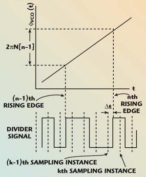
A key design issue in sigma-delta fractional-N synthesizers is utilizing the divider output signal to drive the sigma-delta modulator. As a result, variations in the divide ratio N+dN(t) (where dN(t) is the output of the sigma-delta modulator with an average value equal to the fractional portion of the divide ratio) coincide with the rising edges of the divider signal. This fact poses a difficulty in simulating fractional-N synthesizers since the divider signal has a time-varying period Tdiv that is typically not a multiple of the simulation time step TS. Since the simulated VCO/divider model calculations are based on integrating the divided VCO phase variations, uniform time-step integration will not generate the required accuracy and lock-time behavior.
One way to resolve this problem is to decrease the simulation time step TS (that is increase the sampling rate) indefinitely until the required accuracy is obtained. However, this approach clearly suffers from two major drawbacks: first, the simulation run time becomes prohibitive; secondly, the accuracy clearly becomes a function of the sampling rate. This renders this brute-force approach ineffective.
A much more effective approach is when the exact (continuous) timing of the rising edges of the divider are identified using a key fact3 that those rising edges occur each time the VCO phase advances by 2πN[k], where at any given time, N[k] refers to the value of the divide ratio right before a new rising edge of the divider signal occurs. Once the exact timing of the consecutive rising edges of the divider is obtained, it can be utilized to compute the output of the combined VCO/divider using a non-uniform time-step integration of the divided VCO phase. In what follows, the equations for the proposed scheme are derived.
The output phase of the VCO, ![]() VCO(t), is given by
VCO(t), is given by

where
fo = nominal VCO frequency
K = tuning voltage gain in Hz/V
Vin(t) = tuning voltage input to the VCO
PNVCO(t) = phase noise introduced by the VCO circuit
 | ||
| Fig. 6 VCO phase related to the divider phase. | ||
In Figure 6, tk–1 is the time at the (k–1)th sampling instance, and tk is the time at the (k)th sampling instance. Also, let tn–t be the time instance of the (n–1)th rising edge of the divider signal, and tn be the time instance of the nth rising edge, then according to Perrot, et al.3
![]()
with the initial condition ![]() VCO(t0) = π and N[n–1] corresponds to the division factor that occurs between the (n–1)th rising edge and the nth rising edge of the divider output signal. It can be seen from the diagram of the sigma-delta synthesizer that this division factor remains constant in between two consecutive rising edges of the divider signal. Using linear approximation over the duration ∆t gives
VCO(t0) = π and N[n–1] corresponds to the division factor that occurs between the (n–1)th rising edge and the nth rising edge of the divider output signal. It can be seen from the diagram of the sigma-delta synthesizer that this division factor remains constant in between two consecutive rising edges of the divider signal. Using linear approximation over the duration ∆t gives

where
Ts = simulation time step
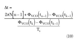
From Equations 8 and 9, ∆t can be solved as

In the above equation, N[n–1] is a known quantity; ![]() VCO(tn–1) is calculated recursively using a discrete version of Equation 7 with the initial condition
VCO(tn–1) is calculated recursively using a discrete version of Equation 7 with the initial condition ![]() VCO(t0) = π, and
VCO(t0) = π, and ![]() VCO(tk) and
VCO(tk) and ![]() VCO(tk–1) are also calculated recursively using Equation 7. Therefore, ∆t can be determined at the rising edges of the divider.
VCO(tk–1) are also calculated recursively using Equation 7. Therefore, ∆t can be determined at the rising edges of the divider.
If the divider signal at the (k–1)th and kth sampling instances is denoted as ![]() div(tk–1) and
div(tk–1) and ![]() div(tk), respectively, then the following nonuniform time step integral recursive expression for the divider phase at kth instance can be obtained.
div(tk), respectively, then the following nonuniform time step integral recursive expression for the divider phase at kth instance can be obtained.

where
PNdiv(tk) = phase noise contribution from the frequency divider circuit at the sampling instance tk
Simulation Results
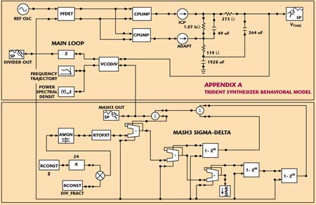
A complete Motorola RFIC fractional-N synthesizer with a third-order sigma-delta architecture was implemented in Ansoft Designer, as shown in Appendix A. The main loop shown at the top portion of the schematic includes the reference oscillator, PFD, charge pump, loop filter and the combined VCO/divider models. The lower portion depicts a digital sigma-delta architecture (MASH 1-1-1)4 that outputs the time-varying fractional divide ratios dN(t). Modeling of the multi-accumulator was accomplished using fixed-point DSP blocks with available bit lengths up to 32.
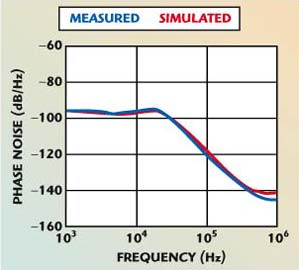
The loop filter topology shown includes an adapt mode input. This topology was utilized to obtain simulated lock-time results, while a narrower bandwidth second-order loop filter without adapt was utilized to obtain the close-in phase noise results. Figure 7 shows the correlation between the measured versus simulated phase noise using Ansoft Designer’s phase noise probe.
 | ||
| Fig. 7 Measured vs. simulated phase noise. | ||
The phase noise probe decimates the incoming phase noise sequence to a rate that matches the maximum frequency offset and then uses FFT spectral estimation using a smaller frequency resolution as the carrier is approached. This enables designers to accurately and efficiently determine close-in and far-out phase noise. Table 2 shows measured and simulated lock times to within ±500 Hz of the final VCO output frequency for frequency jumps of 14 and 30 MHz, respectively.
 | ||
Conclusion
A new simulation tool allows designers to perform detailed fractional-N and integer synthesizer simulations incorporating custom loop filter topologies while determining block-by-block model parameters necessary to meet IC design specifications. The parameter entries used throughout this project reflect both measured and simulated (SPICE) data from the Motorola Tomahawk-II synthesizer IC. It has been demonstrated that given accurate design parameters for each block in the synthesizer, Ansoft Designer is able to closely predict the actual lock-time and close-in phase noise performance.
Acknowledgment
The authors would like to acknowledge the assistance of Mike Schulze and Armando Gonzalez from Motorola for providing SPICE simulations of the charge pump circuitry and measurements of lock-time and close-in phase noise data for the overall fractional synthesizer IC.
Motorola and the stylized M logo are registered with the US Patent and Trademark Office. All other product or service names are the property of their respective owners.
References
- C. Hawang and Y. Lee, “Multifrequency Pade Approximation Via Jordan Continued-fraction Expansion,” IEEE Transactions on Automatic Control, Vol. 34, No. 4, April 1989.
- U.L. Rohde, RF/Microwave Circuit Design for Wireless Applications, John Wiley & Sons Inc., New York, NY 2000.
- M.H. Perrott, M.D. Trott and C.G. Sodini, “A Modeling Approach for Sigma-delta Fractional-N Frequency Synthesizers Allowing Straightforward Noise Analysis,” IEEE Journal of Solid State Circuits, Vol. 37, No. 8, August 2002.
- B. Miller and R.J. Conley, “A Multiple Modulator Fractional Divider,” IEEE Transactions on Instrumentation and Measurement, Vol. 40, No. 3, June 1991.
- W.F. Egan, Frequency Synthesis by Phase Lock, Second Edition, John Wiley & Sons Inc., New York, NY.
Wael A. Al-Qaq earned his BSEE, MSEE and PhD degrees in electrical engineering from North Carolina State University, Raleigh, NC. In 1994, he joined Ansoft Inc., where he is a group leader responsible for the design, development and release of several versions of the system simulation product.
JianHua Gu earned his BSEE degree from Xi’an JiaoTong University, Xi’an, China, in 1994, his MEng (EE) degree from the National University of Singapore in 1998, and his MSEE degree from Mississippi State University in 2000. He joined Ansoft Inc. in 2000 and is currently working in the company’s system group specializing in behavioral mixed signal simulation.
William J. Martin received his BSEE degree from Florida Atlantic University, Boca Raton, FL. He is a member of the technical staff in the CGISS (Commercial Government & Industrial Solutions Sector) Advanced Development organization, Plantation, FL. He was the recipient of the CGISS Regional 1990 and 2003 Patent of the Year Awards.
Jeffrey L. Cutcher received his BS and MS degrees in electrical engineering from the New Jersey Institute of Technology, Newark, NJ. In 1995, he joined Motorola Inc., Plantation, FL, where he worked within the Commercial, Government and Industrial Solutions Sector (CGISS) on next generation public safety mobile radio design. In 2003, he joined the Advanced Technology Team that is part of the iDEN Subscriber Group of GTSS.
