
OEMs, operators and manufacturers of base station RF power amplifiers are constantly striving for greater efficiency, whether it be in the number of connections (calls) that can be made via a base station or the amount of DC power needed to make those calls. For both scenarios, the RF power amplifier plays a key role. First, it is the part of a base station that consumes the most DC power in order to generate the substantial amount of RF power required to maintain a reliable wireless connection for many users. Second, the linearity of the power amplifier determines how many calls can be handled reliably without creating significant interference in neighboring channels in the assigned frequency bands. Today, laterally diffused metal oxide semiconductor (LDMOS) technology is the choice for base station RF power amplifiers because it is reliable, and meets current market needs for performance and cost, with even greater performance improvements possible if the LDMOS technology is further refined.
Common techniques to improve efficiency at the power amplifier level are the Doherty principle, (digital) pre-distortion and, in the case of multicarrier amplifiers, a feedforward concept. What is paramount, however, is to ensure that the RF power amplifier delivers the required base performance. This article describes the trade-offs between linearity, gain and efficiency that can be made for state-of-the-art LDMOS technology.
Amplifier Parameters
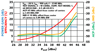
In order to meet the stringent linearity requirements, base station RF power transistors are operated at a much lower power level compared to their actual power capability. This is because most system standards use modulation schemes where the peak power levels are much higher than the average output power. For an EDGE GSM system, for instance, the peak-to-average-ratio (PAR) is a little over 3 dB. For WCDMA systems, it can vary between 6 and 10 dB, or even higher in the case of multicarrier amplifiers, depending on how capable the software algorithms are in reducing the crest factor. Figure 1 shows the continuous wave power capability of a 100 W WCDMA (UMTS) LDMOS transistor1 that uses the current technology. Power gain and drain efficiency are shown.
 | ||
| Fig. 1 CW power capability of a 100 W WCDMA LDMOS transistor. | ||
At Pout = 100 W the power gain compression is 1 dB. Theoretically, considering a PAR of about 6 dB, and in order to avoid significant distortion under WCDMA signal conditions, the device can be operated at a power level of approximately 25 W. Where the device efficiency is 50 percent at 100 W, at 6 dB back-off, it is about 26 percent. For previous generations of LDMOS the efficiency would be around 18 percent. Even with a higher PAR, the device is still able to meet the linearity requirements and maintain good drain efficiency.
Typical linearity requirements under a two-carrier WCDMA signal (PAR = 8.5 dB at 0.01 percent probability of the cumulative distribution function (CDF), that is the chance that a peak 8.5 dB above the average output power will occur) are –40 dBc for the adjacent channel and –37 dBc for the intermodulation distortion (IMD) product generated by the two carriers. Figure 2 shows the two-carrier WCDMA performance for the same transistor.1 The linearity requirements are met at an RF output power of 43.6 dBm (approximately 23 W). Obviously the relationship between the average output power and PAR does not hold up for the full 100 percent, since 43.6 dBm plus a PAR of 8.5 dB adds up to 52.1 dBm, which is well beyond the P1dB capability of the device.
 | ||
| Fig. 2 RF performance of a 100 W LDMOS transistor with two WCDMA carriers at 2140 MHz. | ||
The other parameter that is important in order to meet a particular linearity, in conjunction with the probability on the CDF of the presented input signal, is the peak power capability of the LDMOS transistor. Appendix A presents the peak power capability of the featured LDMOS transistor, where a pulsed continuous wave signal is used with a small duty cycle (about 0.8 percent) to measure the peak power.
It could be argued that it would make more sense to choose the duty cycle such that the average power under pulsed conditions would be more representative of the actual average WCDMA power, which would actually lower the reported peak power capability. It cannot be said that there is a 100 percent correlation between peak power capability of a transistor and achievable linearity. The fact is, though, that a higher peak power capability will reduce the amount of clipping of signals with high peak-to-average ratios, and thus create a transistor that will better fit in a base station amplifier system environment.
Amplifier Efficiency
Having identified the important RF parameters of a UMTS LDMOS base station amplifier, the overall benefit of better LDMOS technology can be determined. Figure 3 shows a block diagram of a UMTS amplifier arrangement using two of the featured 100 W devices in the final stage, driven by a 30 W LDMOS transistor. Figure 4 presents a similar arrangement, now using a previous LDMOS generation in the final stage.2 Both are tested with a two-carrier WCDMA signal, and in both cases the amplifier needs to meet an IMD requirement of –37 dBc and an adjacent channel power ratio (ACPR) of –40 dBc.
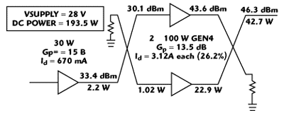 | ||
| Fig. 3 UMTS arrangement with the improved LDMOS devices. | ||
It can be seen from these last two figures that the current technology devices are 6.7 percent more efficient under two-carrier WCDMA conditions. It can be concluded that an amplifier with such LDMOS technology draws about 2.2 A (or 61.6 W DC input power at Vsupply = 28 V) less current for the same output power and same linearity. Most of the improvement comes from the inherently more efficient final stages.
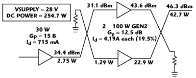 | ||
| Fig. 4 UMTS1 arrangement with a previous LDMOS generation. | ||
The lower gain for the previous generation LDMOS results in the need for a higher output power for the driver transistor, although the increase in current is minimal. With the latest LDMOS, the overall amplifier efficiency is 22 percent, where previously it was 16.8 percent. As a result of this efficiency improvement, the dissipated power is reduced, which is a benefit with respect to heatsink design and/or reliability of the amplifier.
LDMOS Technology Optimization
The majority of the improvements outlined can be found in a proper design of the gate shield, as well as proper drain and gate engineering of the LDMOS structure. However, there needs to be caution, since alterations to these parts of the LDMOS structure may have a negative impact on hot carrier degradation (resulting in Idq drift), breakdown voltage (resulting in a degraded ruggedness) and current capability, as well as drain-source on-resistance (Rds-on) that can effect the peak power capability of the transistor.
Figure 5 depicts a cross-section of the state-of-the-art LDMOS technology. It consists of a silicided poly-silicon gate, a laterally diffused p-well, a p-sinker to connect the source to the highly doped substrate and a lowly doped drain extension region to accommodate high voltage operation. If the drain extension is uniformly doped and optimized for maximum output power, hot carrier degradation will occur, which manifests itself by drift in the quiescent current (Idq) at constant Vgs. A step-wise doping profile, that is two lowly doped regions in the drain-extension (LDD1 and LDD2),3 solves this problem at the cost of some RF performance.
 | ||
| Fig. 5 Typical cross-section of a state-of-the-art LDMOS technology. | ||
However, the introduction of a dummy gate as the shield4 gives a better trade-off between Idq degradation and RF performance. Due to the close proximity of the shield to the gate and drain extension, the field distribution in the drain extension improves, reducing both degradation and feedback capacitance. Another trade-off now becomes dominant — that between the breakdown voltage (BV) and the current capability (Idsx) and on-resistance (Ron).
 | ||
| Fig. 6 Cross-section of stepped shield with highly doped drain region. | ||
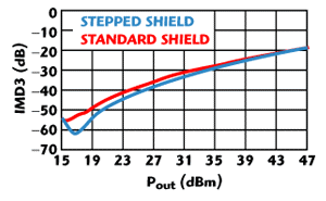
Figure 6 shows a novel stepped shield structure, which combines the advantages of the improved field distribution with a better current capability and Ron. The step construction diminishes the pinching action of the shield near the channel giving an improved Ron and Idsx (see Figure 7), while BV is unaltered due to the action of the lower part of the shield. Figures 8 and 9 show the two-tone large signal RF performance. At linear operation, at –40 dBc IMD3, the output power increases by 1 dB. The linearity-efficiency trade-off is also improved by this novel stepped shield (+ 2 percent efficiency).
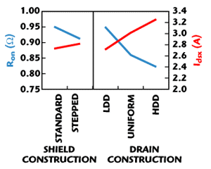 | ||
| Fig. 7 Measured Ron and Idsx for the two shields and three extensions constructions. | ||
 | ||
| Fig. 8 IMD3 vs. Pout for a transistor with Wg = 18 mm, Vds = 26 V, f = 2.15 GHz and ∆f = 100 kHz. | ||
 | ||
| Fig. 9 Measured IMD3 vs. efficiency for standard and stepped shields. | ||
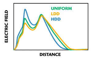
Furthermore, now that an LDD1-LDD2 profile is no longer needed to keep hot carrier degradation in control, it is advantageous to use a more heavily doped drain region (HDD) locally, as shown in Figures 6 and 10. Usually a higher drain doping means a lower BV. However, when the HDD region is properly designed, the peak field in the remaining drain extension does not change (see Figure 11) and the BV remains unaltered. Also, the higher doping concentration has a large impact on Ron and Idsx (see Figure 7). Both improve significantly with the use of an HDD. Figures 12 and 13 show the two-tone large signal RF performance. At around –40 dBc IMD3, the output power increases by 2 dB, while the efficiency also improves by 4 percent. With the higher doping, the feedback capacitance increases, although this is limited to low voltage.
 | ||
| Fig. 10 Doping profiles along the surface of a drain extension. | ||
 | ||
| Fig. 11 Electric field distribution at 26 V along the surface in the drain extension region. | ||
 | ||
| Fig. 12 Measured IMD3 performance of an 18 mm device with different drain extensions at f = 2.15 GHz, Vds = 26 V and ∆f = 100 kHz. | ||
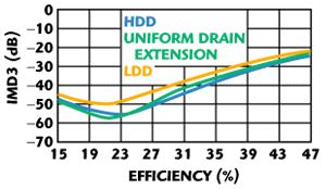 | ||
| Fig. 13 Measured IMD3 vs. efficiency for different drain extensions. | ||