 | |||
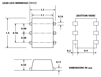
Key considerations when considering low noise amplifiers (LNA) for mobile applications include small dimensions, and low voltage operation and current consumption, allied to excellent electrical performance. Designed to meet these criteria is a new LNA based on the uPC8211TK IC that can be matched with external passive components for different communication bands. It is a SiGe, monolithic integrated circuit packaged in a 6-pin leadless minimold package suitable for surface mounting. As can be seen in Figure 1, it meets the first criteria by being extremely small, making it ideal for mobile applications.
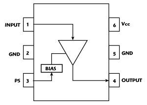
Originally intended as an LNA for GPS applications the IC consists of a single transistor amplifier stage combined with bias circuitry, as shown in Figure 2. As the RF transistor is not matched internally, however, it is possible to match it to different frequency bands for various applications. Therefore, it can cover the frequency range from 400 MHz (for example, for TETRA) up to 2 GHz (W-CDMA), although matching to even lower frequencies is possible.
 | ||
| Fig. 1 Mechanical dimensions of the uPC8211TK IC | ||
 | ||
| Fig. 2 The IC’s circuit configuration. | ||
Even though the bias current cannot be set externally, the achieved linearity of the IC may determine the application in the field. In addition, it is recognized that while an OIP3 of around +6 dBm is not sufficient for some applications, if this specification is not critical then there are the advantages of high gain, low current consumption and power-off functionality. The IC also features a power shutdown pin for easy switch off when not in use, which operates by connecting this pin to ground. In this case, the current consumption can be reduced to a maximum of 1 µA.
Recommended GPS Set Up
Figure 3 shows the recommended set up for GPS. The topology is split into input match, output match and biasing/stability improvement sub circuits. The input match and noise figure are quite sensitive to the values and positioning of the input matching elements (1.3 pF to ground/4.7 nH). At the output there is a parallel combination of resistor (750 Ω) and inductor (22 nH).
 | ||
| Fig. 3 The recommended configuration for GPS usage. | ||
Although the inductor is used to bias the transistor, the resistor loads the output via the 0.1 µF capacitor to ground and reduces the gain to increase the stability of the circuit. Also, the inductor (8.2 nH), in series with the DC block capacitor, forms the output match. With this set up, a noise figure of 1.3 dB and a gain of 18.5 dB are achieved, while current consumption is 3.5 mA at a Vcc of 3 V.
Features and Performance
To expand the capabilities of this unmatched IC to other frequencies and applications, the device was measured on a network analyzer without any matching elements, but with the output resistor and biasing inductor remaining. Using the measurement file in touchstone format (.s2p), a small signal simulation was employed to match the device to other frequencies. Additionally, a resistor was connected in parallel to the one already included in the measurement file to control the gain and therefore the stability of the circuit. From this simulation, a new final real resistor was calculated for use in the circuit for the appropriate frequency.
The topology that was used is the same as in the recommended GPS circuit, but a capacitor from the output to ground is added. The value of each element is different, depending on the frequency, and is given in Table 1, while Table 2 shows the measured performance of the device at all of the simulated frequencies.
| |||||||||||||||||||||||||||||||||||||||||||||||||||||||||||||||||||||||||||||||||||||||||||||||||||||||||||||||||||||||||||||||
As for the noise figure, in order to achieve the optimum for each frequency, it was necessary to make slight adjustments to the input elements. This was achieved experimentally by using a real board and tuning the simulated values of the input matching element until the lowest noise figure was reached.
| |||||||||||||||||||||||||||||||||||||||||||||||||||||||||||||||||||||||||||||||||||||||||||||||||
All Frequencies
The matching topology is the same for all frequencies, which means for each of the five example frequencies there are different values for the matching elements. Figure 4 shows this topology. The pin connected to VPS is the power shutdown. If it is connected to Vcc, the IC is powered on. The two tables show the required values for the matching components to achieve the stated results. As has been mentioned, these values were found by simulation and optimized by experiment.
 | ||
| Fig. 4 The basic circuit topology. | ||
Referring again to Table 1, not only are the matching elements (C2, C5, L1, L3) changed, the resistor R1 varies with frequency. This is mainly done to provide stability because the IC exhibits increased gain at lower frequencies, and therefore, R1 needs to be decreased to maintain stability. It can also be seen that for the recommended circuit for GPS usage, the value of R1 is somewhat lower.
From the simulation it was ascertained that the stability factor can be improved slightly, and therefore, the value of R1 was decreased, with some adjustment to other matching elements also being necessary. The result is high stability with a trade-off towards gain compared to the recommended circuit. Therefore, a LNA designer must decide case by case which version he/she prefers or is better suited to the specific application with regards to stability, and make the appropriate trade-offs.
Measurement Results
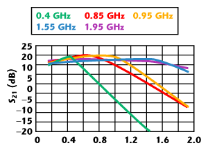
Figure 5 shows the transmission factor (S21) for each matching set up. It demonstrates that the resulting gain maxima drop down at either end of the frequency range. At lower frequencies, the maximum gain coincides well with the intended frequency, exhibiting broadband gain characteristic for the higher frequencies with a more subdued peak at the lower frequencies.
 | ||
| Fig. 5 The transmission factor (S21) for each matching configuration. | ||
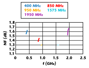
Figure 6 shows the measured noise figure respective to each circuit. It can be seen that the noise figure is lowest for GPS, and for the other frequencies it should also be good enough for most applications.
 | ||
| Fig. 6 The noise figure for each circuit configuration. | ||
