The last few years have seen the manufacturers of chips for short range devices (SRD) operating in the ISM frequency bands (315, 433, 869 and 915 MHz) significantly improving their products. Alongside this, SAW device manufacturers have been endeavoring to develop products offering the best solutions in terms of performance, cost, size and integration of the filtering solutions. To illustrate the work that has been done in this field, this article examines the different methods of improving the RF design of ISM transceivers using these new SAW RF filtering techniques.
Pin-out Architecture
Some chip manufacturers providing products for short range devices have chosen to use a balanced configuration for their low noise amplifier (LNA) receiver. This approach has been widely used in mobile phone architecture, where the LNAs of RF ASICs are differential. The reasons for this choice are technological (the use of a standard amplifier library design) as well as technical, namely, the suppression of common mode noise. These differential LNAs offer an optimum common-mode rejection ratio (CMRR), K = CMRR = 20 log(Ad/Ac), where Ad is the differential mode gain of the device and Ac is its common mode gain. However, in general, using a differential LNA leads to the use of a transformer and impedance networks that split the received signal, the standard architecture for which is the configuration shown in Figure 1.
 | ||
| Fig. 1 Receiver stage using a single-ended filter and a balanced LNA. | ||
By using a balanced output SAW filter instead of a single output one, the RF designer can suppress the use of the transformer and impedance networks (see Figure 2). In addition, the differential architecture of the device suppresses the parasitic capacitance effects of the SAW package, which are compensated for in phase and amplitude. Figure 3 shows the difference between an unbalanced output filter and a balanced output filter.
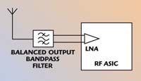 | ||
| Fig. 2 Receiver stage using a balanced filter and LNA. | ||
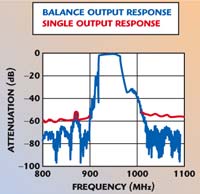 | ||
| Fig. 3 Balanced vs. single output filter responses. | ||
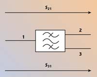 | ||
| Fig. 4 S-parameters of a balanced filter. | ||
When choosing a balanced SAW filter, the engineer must pay attention to the phase and amplitude imbalance specification. A balanced output filter has two propagation paths characterized by S21 and S31, as shown in Figure 4. Ideally, as the SAW filter is a passive component:
|S21| = |S31|
–S21 = –S31 + π
In reality, the physical path differences and the ground defects mean that these equations are not entirely satisfied. In general, the maximum amplitude imbalance can be considered to be approximately 0.5 dB, with a phase imbalance ranging from 2° to 10°, depending on the design technique used by the SAW device manufacturer. These parameters (rejection level of the balance filter, imbalance and CMRR) do have a significant impact on the sensitivity of the receiver module.
Size and Cost Reduction
When designing an ISM transceiver for alarm, meter-reading or remote control systems, the two main constraints encountered, other than technical, are the cost and reduction of the size of the module. The majority of RF engineers recognize that efficient filtering is the key to avoiding transmission problems. However, filtering has a cost, and the price of the complete module might be a critical issue.
The latest packaging technologies that were initially developed for mobile phone communications will help engineers to solve the designer dilemma shown in Figure 5. Obviously, the cost of the SAW filter varies with the size of the device, with the filter getting cheaper as the size decreases.
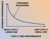 | ||
| Fig. 5 Size and cost vs. electrical performance of a SAW filter. | ||
Equally, the main cost of a SAW filter is packaging, typically representing 60 to 80 percent of the total cost of the filter. The main reason being that packaging is a unitary process, whereas SAW manufacturing is a total one because it uses wafer foundry technology. With up to 5000 devices being processed on a single wafer simultaneously, the die cost is driven down dramatically.
A new packaging technology, commonly known as chip scale packaging (CSP), has been developed. The advantages are that whereas standard surface mounted device (SMD) technology is limited to a minimum size of 3 x 3 mm, CSP technology enables filters as small as 2 x 1.4 mm, and even 1.6 x 1.4 mm, to be produced. In addition, as CSP technology is not a unitary process, the price of the single packaged device is reduced. Appendix A details the characteristics of the different technologies.
Using CSP technology is claimed to produce a 70 percent size and 20 percent cost reduction compared to the standard 3 x 3 mm SMD technology and a solution to the RF designer dilemma (see Figure 6). For a given filtering performance FP1, the CSP technology is a cheaper and smaller solution.
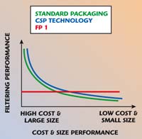 | ||
| Fig. 6 CSP packaging vs. standard packaging technologies. | ||
SAW Integration
Recently, some alarm manufacturers have used the argument of security and reliability for proposing a technology using two different frequencies. In Europe, both the 433 and 869 MHz frequency bands are jointly used inside the new alarm bases, negating the effects of interference. Basically, if the base cannot identify the alarm signal at one frequency due to interference, it will switch to the other frequency. There have been requests to integrate both 433 and 869 MHz filters inside the same package; therefore, 4 x 2 mm dual SAW filters are being developed.
On the other hand, some worldwide companies supply their transceivers to both Europe and the US. European RF modules commonly use the 869 MHz frequency, whereas the US modules are developed at 915 MHz. Today, most of the ISM chipsets can cover a frequency range from a few megahertz up to 1 GHz. As a result of these developments, stock management and economies of scales are possible and companies will be able to switch their production from one regional location to another depending on the prevailing economics.
Different approaches can be taken in order to design the dual SAW. Either the two filters can be designed on separate dies, or grouped, where possible, on a single die (see Figure 7). The advantages of the latter are the ability to use the same metal thickness for both structures, because they are processed together on the same wafer, and to achieve smaller devices. Consequently, the cost of a dual SAW filter is lower than for two separate packaged devices.
 | ||
| Fig. 7 Dual SAW filter integration; (a) single or (b) double-die. | ||
Electrical Performance
Generally, short range devices take the low power module approach, because when in the receiving mode, SAW filters do not have to withstand very high powers. In fact, most of them are effectively specified to withstand less than 10 dBm input power. However, in a transceiver module, a SAW filter withstanding 17 dBm (500 mW with 10 percent duty cycle, corresponding to an effective power of 50 mW – class 12 of ETSI SRD description) will enable the same device to be used for both transmission and reception (see Figure 8).
 | ||
| Fig. 8 SAW filter used in reception and transmission. | ||
As an example of how products have been developed, Temex SAW filters in the ISM range are all designed to withstand 27 dBm, although they are generally specified at 17 dBm, which is generally the power limit in the range of 30 to 1000 MHz. Here, a standard test, where the SAW filters are submitted to 27 dBm CW for 1000 hours, at maximum temperature (generally 80°C), is undertaken, and must show no change in the performance of the device.
For the SAW device to withstand high powers is a question of mastering the metal deposition process. Different layers of metal (aluminum and others) are disposed in a way that does not allow the atoms of the structure to migrate when high power is applied. For two-way communications applications, such as meter-reading, home automation, and in some cases, alarms, there are benefits, in terms of cost, size and integration.
Tailored Rejections
With standard RF transceiver designs using a 10.7 MHz bandwidth, it is possible, for instance, to use a tailored RF SAW having notch resonators placed at the dedicated frequency. Figure 9 shows a filter that uses these techniques to avoid the 10.7 MHz IF interference. In conjunction with this, a different notch technique will provide 70 dBm rejection or more at the GSM frequency band.
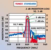 | ||
| Fig. 9 Design techniques for short range device SAW filters. | ||
In both cases, the layout of the test board is key in order to take advantage of these techniques as any parasitic effect added from the board would destroy the notch trap. Isolation between input and output ground, for example, is essential.
All the parameters described have a strong influence on the signal-to-noise ratio, spurious response rejection, intermodulation response rejection, blocking and desensitization. 70 dB is a common rejection level to reach. SAW filters will enable those levels to be achieved, while keeping the linearity of the system immune, with losses as low as 2 dB within the passband.
