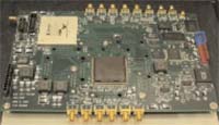
Digital RF memories (DRFM) are used for the reproduction of complex, coherent signals usually associated with modern pulse compression radars. There are many different implementations of DRFM systems. Figure 1 displays one particular type, a double sideband, four-bit, phase sampled system with 500 MHz of instantaneous bandwidth.

Fig. 1 DRFM baseband processor with LNX digital RF memory and external memory interface.
A custom mixed signal application-specific integrated circuit (ASIC) was designed and fabricated in 0.18 µm CMOS that implements the baseband components of the system including the phase-sampling circuit, digital processing, signal reconstruction and digital-to-analog outputs.
ASIC Design
A block diagram of the LNX DRFM ASIC is shown in Figure 2. A preamplifier stage amplifies, buffers and level shifts the input to facilitate the interface to the digital logic circuitry. The input bandwidth is 250 MHz providing 500 MHz of instantaneous bandwidth using the I and Q inputs. High speed comparators are used to sample the I and Q inputs at up to 640 MHz, while a look-up table is used for error correction and encoding into a four-bit phase value representing 22.5° of resolution. Data is then stored for processing and playback. The signal is reconstructed using the phase data and sine/cosine look-up tables.

Fig. 2 Simplified block diagram of the LNX DRFM ASIC.
After encoding, the data enters a demultiplexing block where it is distributed over a 20-bit bus that runs at one quarter the sampling rate, facilitating storage in an external memory. Alternatively, the data is fed to the next delay line block. This block implements two functions: it can either delay the digitized signal in fixed increments or it can recirculate the data for head-to-tail reconstruction. Head-to-tail reconstruction or recirculation allows a CW signal to be replayed with the correct phase and frequency characteristics of the recorded signal. The minimum throughput time delay is < 25 ns.
The external memory interface operates at 160 MHz and performs the demultiplexing for data storage and playback. Full duplex operation allows signals to be sampled and stored simultaneously with the playback and transmission of a previously stored signal. Data signal levels are 3.3 V CMOS and the clocks are differential LVDS. The ASIC supplies all of the timing and control for external storage. An external memory, FPGA or DSP processing system can be used to store and/or process the recorded waveforms.
The ASIC contains all of the timing necessary to maintain phase coherency for signals that are recirculated. Timing is also provided to external circuitry to maintain the coherence of recorded signals. The timing circuitry can also be used for range gate pull off (RGPO) in radar jamming applications. In this scenario, the jammer can walk the range gate of the radar off the target.
There are other auxiliary circuits such as a pseudo-random noise (PN) generator and a frequency measurement function. The PN noise generator can be used to add pseudo-random noise to the output signal. The frequency measurement block can measure the frequency of the input signal with up to 10-bit accuracy using accumulated delta phase measurements; the resolution of the frequency measurement can be automatically adjusted depending on pulse length.
A microprocessor interface is provided for configuration and test. For example, data can be written to, or read from the external memory interface from the microprocessor bus. Status and control registers are also provided.
The back end of the ASIC implements a quadrature modulator. Independent sine/cosine look-up tables convert the four-bit phase values to sine/cosine outputs. Two on-board digital-to-analog converters convert the look-up table outputs to analog outputs for signal reconstruction and up-conversion. The update rate of the D/A is 640 MHz, consistent with the sampling rate and is capable of driving ±0.5 V into 50 Ω.
Performance
Performance of the new chip met or exceeded all of the requirements. The chip displayed < 5 mV of input offset, with an input bandwidth of > 250 MHz and a clock frequency of > 700 MHz. Figure 3 shows signal reconstruction and playback of a 2 MHz input signal sampled at 730 MHz. The device is operating in recirculate mode where a sampled pulse is being reconstructed in a head-to-tail fashion, with no phase discontinuity.

Fig. 3 Reconstruction of a 2 MHz signal sampled at 730 MHz in recirculate mode.
Other performance characteristics include four-bit (22.5°) phase resolution and < 25 ns throughput delay, with multiple delay modes, phase and PN noise modulation, 10-bit frequency measurement capability, and multiple target tracking. The ASIC features a 160 MHz external memory interface and a dual-channel, four-bit digital-to-analog converter for signal reconstruction. Power dissipation is 2.5 W and the operating temperature range is –40° to +85°C. The IC is housed in a 240-pin CQFP package.
Conclusion
A mixed-signal ASIC has been introduced for digital RF memory applications. The device includes preamplifiers, phase sampling, an external memory interface and signal reconstruction. It is implemented in 0.18 µm CMOS and features an instantaneous input bandwidth of > 500 MHz and phase data sampling at 640 MHz. The ASIC includes all of the timing and control for phase coherent external data storage and signal reconstruction, signal delay and recirculation, pseudo-random noise generation, and frequency measurement. The architecture of the device is particularly aimed at DRFM applications.
LNX Corp.,
Salem, NH
(603) 898-6800,
www.lnxcorp.com.
