Due to the fast development of wireless communications, a low cost, high performance, highly integrated technology is needed for system-on-a-chip (SoC) implementations. The CMOS technology provides a good solution for SoC integration.1 Recent improvements of the standard CMOS process make it possible to implement RF blocks, such as low noise amplifiers, mixers, voltage-controlled oscillators (VCO), power amplifiers and T/R switches,2,3 for operation at frequencies in the 2.4 and 5 GHz bands. Also, a 2.4 GHz CMOS power amplifier with an output power of 20 dBm has recently been reported.4 The goal of a single-chip transceiver radio or a radio-on-a-chip (RoC) with a medium-range transmitting power has become more feasible.

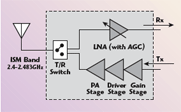
In this article, a 2.4 GHz single-chip CMOS transceiver RF front-end is presented (see Figure 1) for ISM-band wireless applications. The transceiver includes a three-stage power amplifier with a diode linearizer, a series-type T/R switch and a gain-controlled LNA. The RFIC was fabricated with the 0.25 ?m 1P5M standard CMOS process. Using an FR-4 PCB test fixture, extensive measurements were performed in the transmit and receive modes, including the IEEE 802.11b transmit spectrum mask test.
Receive Circuit Design

Gain-controlled LNA
The first and second stages of the LNA use a cascode and cascade topology to increase gain and isolation. The cascode configuration is used to reduce the Miller effect and to increase the 3 dB bandwidth of the amplifier. Owing to the high isolation of the input and output ports of the amplifier, the matching task can be easily done. The schematic of the designed 2.4 GHz CMOS, two-stage, gain-controlled LNA (with a T/R switch) is shown in Figure 2. The design procedure is as follows:
-
The most important procedure is to choose the right NMOS transistor channel width, which has the lower noise figure.5 In accordance with the simulation results, the channel width of the first NMOS transistor was chosen to be 160 ?m.
-
On-chip spiral inductors were used for the RF chokes of the first and second stages. The RF chokes have been chosen from experience to provide a good inter-stage matching of the two stages.
-

Due to the low Q-factor and the large size of the chip spiral inductors, off-chip lump elements are used to realize the output matching circuit.
-
The input port of the LNA and the Rx port of the T/R switch are connected on chip. The interface between the T/R switch and LNA is designed to be conjugately matched.
-
A gain control circuit is added by using a parallel variable resistance, which is implemented by using a NMOS transistor biased at Vds = 0 V.6
Series-type T/R Switch

Two typical circuit configurations of the T/R switch, the series- and shunt/series-type switches, are shown in Figure 3. Adding the two shunt arms to a series-type T/R switch forms the shunt/series-type T/R switch. The two shunt arms increase the isolation between the Tx and Rx ports of the shunt/series-type T/R switch over that of the series-type. Although a low isolation could possibly saturate the received signal with the transmit signal leaking when the PA is turned on, for WLAN applications (with a TDD duplex) when the Tx and Rx modes will not turn on simultaneously, the series-type T/R switch should be adequate. In addition, the series-type T/R switch has a lower insertion loss, a simpler architecture and no power consumption. Here the series-type T/R switch is used for integration into the designed 2.4 GHz transceiver RF front-end circuits. The design considerations are as follows:
-
As shown in Figure 4, when the transistor is turned on and off, it can be modeled as a resistor R and a capacitor C. The resistor R results in an insertion loss when a signal passes through the transistor; the capacitor C provides the isolation between the two ports of the transistor.
-

When the transistor is turned on, as the transistor gate width is increased, the on-state resistance R becomes smaller and results in a lower insertion loss.
-
When the transistor is turned off and the transistor gate width is increased, the off-state capacitance C becomes larger and results in a lower Tx/Rx port isolation.
-
By using the above three rules, the most suitable transistor gate width is chosen according to the simulation results from the RF model.
-
The interfaces between the T/R switch, LNA and PA are connected on chip and the antenna port uses an off-chip matching circuit to assure the antenna port is matched to 50 ?.
A series-type 2.4 GHz CMOS T/R switch is shown in Figure 5. A 320/0.24 ?m transistor gate width (Tx arm) and a 90/0.24 ?m transistor gate width (Rx arm) are chosen for the series arms. In order to have a higher PA output power, a larger gate width is chosen for the Tx arm transistor. The control voltage is 2.5 V. Note that a resistance R1 is needed to assure a DC ground-return path. A summary of the simulated characteristics is given in Table 1.

Receive Mode Test
Figure 6 illustrates the receiving mode test for the transceiver RF front-end. Figures 7, 8, 9 and 10 and Table 2 show the simulated and measured performance in the receiving mode. The receiving mode exhibits a gain of 12.9 dB. The noise figure is 5.7 dB. The input 1 dB compression point (P1dB) is approximately –5.3 dBm, and the IIP3 is approximately 1.5 dBm. The input (at the antenna-port of the T/R switch) and output return losses are approximately 12.5 and 23.3 dB. When the gain control circuit turns on at 2.44 GHz the gain tuning range is approximately 12.93 (Vctrl = 0 V) to 2.24 dB (Vctrl = 2.5 V) and the noise figure over the tuning range is approximately 5.7 (Vctrl = 0 V) to 10.35 dB (Vctrl = 2.5 V).

Transmit Circuit Design
Power Amplifier with a Diode Linearizer
In order to decrease the output power required from the upconversion mixer, when the power amplifier (PA) is operated at the maximum output power, the 2.4 GHz CMOS linearized PA requires a three-stage topology. Because of the need for enough linearity, the designed PA uses a class-AB topology and a diode linearizer at the output stage to increase the linearity of the PA.7 Due to the low breakdown voltage and high knee voltage, the output power and efficiency of a CMOS PA is limited. The design goal of the 2.4 GHz CMOS linearized PA (with T/R switch) is: output P1dB > 13 dBm, linear gain > 25 dB, and PAE > 12 percent. The schematic of the designed 2.4 GHz CMOS three-stage, linearized PA (with T/R switch) is shown in Figure 11. The following is the design procedure:

-
A class-AB topology (Vg = 0.9 V) is used at the output stage to acquire enough linearity.
-
The channel width of the output stage transistor is chosen to be 600 ?m, using ADS load-pull software.
-
The driver and gain stages are designed to drive the output stage to the desired output power, and the channel width of the gain and driver stages are chosen to be 90 and 320 ?m, respectively.8
-
A resistor is placed across the gate and drain of the transistors to increase the stability of each stage and assure that the PA is unconditionally stable.
-
In order to prevent metal migration of the on-chip spiral inductors, the RF chokes at each stage use off-chip inductors, and the three RF chokes have been experimentally chosen to provide a good power match of the three stages.
-

The output port of the PA and the Tx port of the T/R switch are connected on chip, and the interface between the T/R switch and PA is designed to be power matched.
-
The input port of the PA uses an off-chip matching circuit to assure the input impedance of the PA to be 50 ?.
Transmit Mode Test
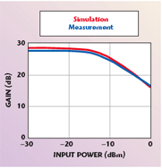
Figure 12 illustrates the transmitting mode test for the transceiver RF front-end. Figures 13, 14, 15 and 16 and Table 3 show the simulated and measured performance of the transmit mode. The transmit mode exhibits a gain of 28 dB, an output 1 dB compression point of approximately 13.5 dBm, an OIP3 of approximately 20.3 dBm and a PAE of 14.9 percent. The input and output return losses (at the antenna-port of the T/R switch) are approximately 16.5 and 7.8 dB, respectively. All the tests were made at 2.44 GHz. The maximum allowable output power is 13.4 dBm for the IEEE 802.11b transmit spectrum mask test (center frequency = 2.44 GHz, Gaussian filter BT = 0.4, data rate = 11 Mbps). Figure 17 shows a micrograph of the 2.4 GHz CMOS transceiver RF front-end RFIC chip with a size of 1.92 × 1.10 mm2.

Conclusion
The design, fabrication and measurements of a 2.4 GHz CMOS transceiver single-chip RF front-end have been presented. The single-chip RFIC, with a chip size of 1.92 × 1.10 mm2, is fabricated with the 0.25 ?m 1P5M standard CMOS process. The transceiver RFIC consists of a series-type T/R switch, a gain-controlled LNA and a three-stage PA with a diode-linearizer. Using an FR-4 PCB test fixture, extensive measurements in the transmit and receive modes were performed, including an IEEE 802.11b transmit spectrum mask test. For the receive mode, the CMOS transceiver RFIC exhibits a gain of 13 dB, a noise figure of 5.7 dB, an input P1dB of –5.3 dBm and an IIP3 of 1.5 dBm. The input (at the antenna-port of the T/R switch) and output return losses are approximately 12.5 and 23.3 dB, respectively. The gain tuning range is approximately 12.93 (Vctrl = 0 V) to 2.24 dB (Vctrl = 2.5 V) and the noise figure within the tuning range is approximately 5.7 (Vctrl = 0 V) to 10.35 dB (Vctrl = 2.5 V), respectively. For the transmit mode, the CMOS transceiver RFIC exhibits a gain of 28 dB, an output 1 dB compression point of approximately 13.5 dBm, an OIP3 of approximately 20.3 dBm and a PAE of 14.9 percent. The input and output return losses (at the antenna-port of the T/R switch) are approximately 16.5 and 7.8 dB, respectively. The maximum allowable output power is 13.4 dBm for the IEEE 802.11b transmit spectrum mask test (center frequency = 2.44 GHz, Gaussian filter BT = 0.4, data rate = 11 Mbps). The CMOS transceiver RFIC performance demonstrates that the standard 0.25 ?m CMOS process has a great potential in the transceivers for 2.4 GHz wireless communications.

Acknowledgments
This work was supported by the National Science Council, Taiwan, ROC, under Grant NSC 92-2213-E-006-063. The authors would like to thank the Chip Implementation Center (CIC) of the National Science Council, Taiwan, ROC, for supporting the TSMC CMOS process.
References
1. T.H. Lee, The Design of CMOS Radio-frequency Integrated Circuits, Cambridge University Press, 1998.

2. K. Yamamoto, T. Heima, A. Furukawa, M. Ono, Y. Hashizume, H. Komurasaki, S. Maeda, H. Sato and N. Kato, “A 2.4 GHz Band 1.8 V Operation Single-chip Si-CMOS T/R-MMIC Front-end with a Low Insertion Loss Switch,” IEEE Journal of Solid-State Circuits, Vol. 36, No. 8, August 2001, pp. 1186–1197.
3. C.C. Yen and H.R. Chuang, “A 2.4 GHz 0.25 ?m CMOS Transmitter and Receiver RFICs for Wireless Communications,” Microwave Journal®, Vol. 38, No. 2, February 2005, pp. 56–76.
4. C.C. Yen and H.R. Chuang, “A 0.25 mm 20 dBm 2.4 GHz CMOS Power Amplifier with an Integrated Diode Linearizer,” IEEE Microwave and Wireless Component Letters, Vol. 13, No. 2, February 2003, pp. 45–47.

5. D.K. Shaeffer and T.H. Lee, “A 1.5 V 1.5 GHz CMOS Low Noise Amplifier,” IEEE Journal of Solid-State Circuits, Vol. 32, No. 5, May 1997, pp. 745–759.
6. “GaAs AGC Amplifier for CDMA Cellular Phone Systems,” OKI Technical Review, Vol. 63, No. 158, April 1997.
7. T. Yoshimasu, M. Akagi, N. Tanba and S. Hara, “An HBT MMIC Power Amplifier with an Integrated Diode Linearizer for Low Voltage Portable Phone Application,” IEEE Journal of Solid-State Circuits, Vol. 33, No. 9, September 1998, pp. 1290–1296.
8. S.C. Cripps, RF Power Amplifier for Wireless Communications, Artech House Inc., Norwood, MA, 1999.

9. F.J. Huang, et al., “A 0.5 ?m CMOS T/R Switch for 900 MHz Wireless Applications,” IEEE Journal of Solid-State Circuits, Vol. 36, No. 3, March 2001, pp. 486–492.
10. A. Zolfaghari and B. Razavi, “A Low Power 2.4 GHz Transmitter/Receiver CMOS IC,” IEEE Journal of Solid-State Circuits, Vol. 38, No. 2, February 2003, pp. 176–183.
Wei-Ting Lee received his BSEE degree from National Sun Yat-Sen University, Kaohsiung, Taiwan, and his MSEE degree from National Cheng Kung University, Tainan, Taiwan, in 2002 and 2004, respectively. He worked on 2.4 GHz CMOS transceiver RFICs for his master study. He currently works for Asus as an RF engineer. His research interests include RFIC and RF system designs for wireless communications.
Huey-Ru Chuang received his BSEE and MSEE degrees from National Taiwan University, Taipei, Taiwan, in 1977 and 1980, respectively, and his PhD degree in electrical engineering from Michigan State University, East Lansing, MI, in 1987. He is currently a professor at the Institute of Computer and Communication Engineering, National Cheng Kung University, Tainan, Taiwan. His research interests include RFIC/RF-SoC and antenna design for wireless communications, computational electromagnetics and its applications, EMI/EMC, microwave communications and detection systems.

Chun-Lin Lu received his BSEE and MSEE degrees from National Chiao Tung University in 1977 and 1979, respectively. He is currently a professor in the department of computer and communication engineering, Kun Shan University, Tainan, Taiwan. His research interests include microprocessor applications, power electronics, wireless communication and RFIC design.


