MMIC processes based on GaAs PHEMT and MHEMT transistors have shown continuous performance improvement over time – meeting the increasingly stringent specifications required by new standards and adapting to the move towards the use of MMICs at higher and higher frequencies. However, even with these performance improvements, it is necessary, in many cases, to develop additional functionality of the MMIC to make a real difference to the final system performance and cost.
For many RF systems it is beneficial to increase the level of integration by including all the RF functions on the same MMIC. For example, the integration of the different elements that make up a T/R module (amplifiers, switches, digital attenuators, digital phase shifters) of a phased array system on to the same MMIC not only simplifies the mounting of the MMIC but also reduces the overall cost.
Also, while being analogue, with regards to RF functions, the digital phase shifter and digital attenuator actually have a parallel digital interface to control the phase and attenuation settings. Unfortunately, the higher level of integration of such functions leads to the need for a much more complex digital interface to a single MMIC. The digital phase shifter and attenuator use a parallel interface - for example 6-bits of phase control requires up to 12 control pads – and the same is true for the attenuator function. This results in a MMIC with many bonding pads, which, in turn, complicates the testing and mounting of the circuit and complicates the interfacing to the MMIC.
Fortunately it is possible to fabricate on chip Serial to Parallel (SIPO) converters that greatly simplify the interface – requiring only three control pads: Data, Clock and Data Ready. The addition of a Data Out enables daisy chaining of the core chips, further reducing the complexity.
The SIPO needs to be robust, independent of temperature and to consume little current. This ideally requires a positive only operation of the transistor – what is called the enhancement mode transistor where the Vt is positive. The amplifier and switching functions can be fabricated using the normal run-of- the-mill depletion mode transistor with its negative Vt.
Incorporating both the enhancement and depletion mode transistors into the same MMIC allows the fabrication of excellent RF functions such as the phase shifters, attenuators and amplifiers using the depletion mode, while at the same time the SIPO is fabricated using the enhancement mode transistor.
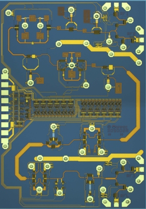
An example of an X-band core chip, including both phase shifters and switches is shown in Figure 1 – this MMIC also includes the SIPO, making it a very easy to implement MMIC. The digital section (the SIPO) requires only 40 mW and can operate at speeds in excess of 200 Mb/s.

Figure 1.
Another Example of including an additional option on the MMIC is the RF MEMS Switch. The ohmic contact RF MEMS switch has very low loss and almost perfect linearity, making it a very useful component in many systems – for example in replacing the transistor based switch in a phase shifter or as a very low loss redundancy switch. To fully exploit the potential of the RF MEMS switch it is necessary to implement the device as close as possible to the other RF functions, for instance placing the Low Noise Amplifiers after a redundancy switch. Any additional losses from the packaging of the RF MEMS or 50 Ω interconnection lines will add directly to the noise figure.
The integration of the MEMS into the same MMIC as the LNA leads to an optimum and high performance redundancy switch and LNA configuration. Figure 2 shows a photo of an integrated RF MEMS. The MEMS device is processed at the same time as the MMIC and can be incorporated into a conventional MMIC, including all the normal passive and active devices. Losses as low as 1 dB at 95 GHz can be achieved using the MEMS switch. OMMIC, together with the other partners of the FP7 MEMS4MMIC project are also developing both Level 0 (on chip) and Level 1 packaging.

Figure 2.
Finally, the market for W-band circuits for passive and active imaging systems is increasing rapidly. These systems require very low noise amplifiers, followed either by down converters or direct conversion using a suitable detector diode.
Unfortunately the interfacing to the RF circuit at 90 GHz is not a trivial task – being both costly and performance limiting. If the RF interfacing is provided on chip via, for example, integrated antennas at the input and detector diodes at the output (providing an IF signal) then the use of the MMIC is greatly simplified, the performance enhanced and the overall cost reduced.
Another important aspect is the performance of the detector diode – low 1/F noise is essential, as high sensitivity and low variation to temperature variations again greatly enhance the performance and simplify the use of the MMIC. Temperature stability is a key factor in reducing the system complexity and requirement for expensive and noisy temperature stabilisation systems.
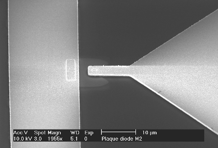
OMMIC has developed a Resonant Interband Tunnel Diode (RITD) that has a low 1/F noise and requires no biasing. In addition the RITD is grown on top of the normal epitaxial layers used for OMMIC’s 70 nm MHEMT process transistor. In the future this will enable the RITD to be used as a detector diode directly before the LNA (with typically 2.5 dB noise figure at 90 GHz). An example of the RITD diode is shown in Figure 3. The DC characteristic in Figure 4 shows the tunnel effect but more importantly the highly non-linear behaviour close to 0 V.

Figure 3.

Figure 4.
This combination of the integration of a robust zero-biased RITD with an excellent LNA MMIC technology will lead to the possibility of manufacturing passive millimetre-wave imaging systems with higher performance, without the requirement for stringent temperature stabilisation and at a reasonable cost.
The above examples show that basic MMIC technology alone is not sufficient – frequently it is necessary to add the right additional processing module to really improve the system performance and also to reduce costs and increase manufacturability. It is important for a foundry to have these additional options built in as modules to the basic technology roadmap. In this way GaAs technologies will continue to be an essential part of the technology landscape for a long time into the future.

