RF and microwave switches based on PIN diodes or GaAs FETs have been key microwave design components for decades, with each type establishing itself in specific applications based on its inherent characteristics. In short, GaAs FETs offer fast switching speed and can operate down to DC, but can handle typically only a few watts of RF power, while PIN diodes can handle much greater power levels, but consume more DC power. Truly high power levels remain the domain of electromechanical switches, which can handle hundreds of watts but are also orders of magnitude greater in size and weight than solid-state switches.
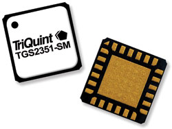
Gallium nitride changes the equation. Having firmly established itself in RF power amplifiers for its ability to deliver higher RF output power than GaAs or silicon (above ?3 GHz) over broader bandwidths, gallium nitride now offers another switching option that provides performance not achievable with other semiconductor technologies. The TGS2351-SM GaN MMIC SPDT switch from TriQuint Semiconductor exemplifies what can be achieved with FET-based GaN MMICs. The reflective switch operates from DC to 6 GHz, can handle up to 40 W CW, switches in less than 35 ns, has insertion loss of less than 1 dB and isolation greater than 40 dB. The product offers a new realm of possibilities for designers addressing defense, aerospace or high performance commercial RF design needs.

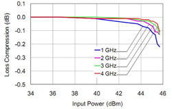
Figure 1 Insertion loss change as a function of input power at four different frequencies.
The high breakdown voltage that is a fundamental characteristic of GaN lends itself well for use in high power RF switches. The high power-handling ability and wide 0/-40 V DC control voltage range of the TGS2351-SM are directly attributable to GaN's high power density, which is also the key to its appeal in RF power amplifiers. The TGS2351-SM is fabricated using the company's 0.25 µm HEMT GaN-on-SiC process. When compared to a FET switch fabricated in a typical 0.25 µm GaAs process, the TGS2351-SM can handle two and a half times the on-state power, eight times the off-state power and is highly stable with little or no performance degradation over temperature. RF power handling ability is shown in Figure 1.
For switch applications, TriQuint's GaN process yields a breakdown voltage of 70 V DC compared to 13 V DC for GaAs and can handle current of more than 1 A/mm of device area versus 650 mA/mm for GaAs. In addition, the high thermal conductivity of the insulating SiC substrate reduces leakage caused by high RF voltage swing while also improving heat transfer to the back of the device. These are compelling metrics when considered in the context of applications such as electronic warfare, radar and high power communications systems.

A FET's main control parameters are its on-state resistance and off-state capacitance that together determine a switches' RF impedance in the two switching states; insertion loss and isolation performance are strongly dependent on them. The TGS2351-SM's on-state resistance is 2.4 Ω-mm and its off-state capacitance is 0.17 pF/mm, which are similar to such specifications achieved by GaAs FET switches. The insertion loss of the switch is less than 1 dB over its frequency range and varies minimally with increases in input power (see Figure 1). Isolation is typically 40 dB and switching speed compares favorably with that of all other types of solid-state switches. Typical performance for the TGS2351-SM is shown in Table 1.
The TGS2351-SM is housed in a 4 × 4 mm, 24-lead, air-cavity QFN package. The air-cavity approach is a proprietary TriQuint process development that utilizes industry-standard ceramic packages to provide enhanced protection for GaN die as well as a means for mitigating high temperatures commonly found in high power GaN devices. The air cavity QFN helps mitigate heat in a way not possible with fully encapsulated plastic packaging alternatives. TriQuint offers full packaging services for its die-level devices through a wide selection of industry-standard form factors. The company also provides custom solutions for unique customer requirements through its Advanced Microwave Module Assembly (AMMA) in-house facilities that deliver secure, one-stop convenience.
TriQuint offers its new GaN switch in die form as the TGS2351, which differs in performance only in its insertion loss, which is less than 0.8 dB. Both devices are members of TriQuint's growing family of SPDT GaN switches that includes the TGS2352 and TGS2353 die-level devices. The TGS2352 operates from DC to 12 GHz, handles up to 20 W CW, has insertion loss of less than 1 dB, switches in less than 25 ns and has isolation greater than 35 dB. The TGS2353 operates from DC to 18 GHz, handles 10 W CW, has insertion loss of less than 1.5 dB, isolation greater than 30 dB and switching speed of less than 25 ns. In the TGS2351-SM as well as the other devices, control voltages are available from either side of the MMIC. Packaged versions of the 12 and 18 GHz die-level devices will be offered in the future.
TriQuint Semiconductor
Richardson, TX
(972) 994-8200
www.triquint.com/defense
