When prototyping RF circuits, it is essential to work in micrometer precision. Even small deviations can lead to undesirable results. Basically, PCBs are manufactured in a negative process: non-conductive regions are removed from a full surface-coated substrate and the conductor structures remain intact.
This conductive layer can be removed by chemical processes such as etching, usually by service providers or in series production. However, when it comes to geometrical precision, rapid prototyping or protecting sensitive data layout, chemical-free methods have significant advantages. This is because the geometry of the generated circuit boards is very similar to the idealized standards of layout and simulation programs. In particular, the higher the transmitted frequencies, the more apparent the impact of variations on the signal quality.
LPKF has been delivering systems for milling PCB prototypes since 1976. The company has upgraded its milling plotters, the ProtoMat family, with additional options that include features that make the plotters particularly suitable for RF applications. They are supplied with a modern soundproof enclosure and, recently developed, easy-to-use software is also included.
All ProtoMats are suitable for structuring classical circuit boards, drilling, depanelling or front panel engraving. The mechanical repeatability is 0.5 microns, with a maximum head speed of 150 mm/s (6 in/s). The work surface accommodates substrates up to 9 × 12 inch (229 × 305 mm).

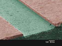
Figure 1 FR4 material processed with a specialized RF tool (End Mill RF).
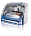
ProtoMat S103
The S3 series plotter can be gradually upgraded one step at a time: From the entry-level S43 to the top of the range LPKF ProtoMat S103, which is the most suitable for RF applications. With a spindle speed of 100,000 rpm, the ProtoMat S103 is able to structure both very hard and sensitive materials and the result is steep edges (see Figure 1), which minimize signal losses. The sectional view (colored) shows the straight walls and low penetration depth.
As has been mentioned, the milling plotters incorporate new, user-friendly LPKF CircuitPro software. With this software, occasional users are guided by wizards through the individual process steps, while more experienced users have individual access to each program option. CircuitPro adopts data from the layout program and prepares it to control the circuit board plotter. A material library with an extensive collection of parameters is included and is used to optimize the structuring results on a material-specific basis. Individual parameters can also be added.

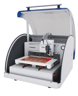
Figure 2 Standard configuration of the ProtoMat S103.
Even in standard configuration the ProtoMat S103 comes with fiducial camera, vacuum table, dispenser and a high performance milling head, as shown in Figure 2. Also, the structuring process of the new plotter is considerably more automated than its predecessor, with the facility to change the necessary tools from a 15-piece tool bank. Any use of the tools is logged, enabling conclusions to be made on the degree of wear.
Another innovation is that the ProtoMat automatically selects the penetration of the tool. This ensures precise milling depth while structuring and results in minimal effects on the substrate during milling. For instance, on 18/18 FR4 material, isolation channels and signal-track width can be implemented safely at 100 microns.
Milling Depth Control
In addition to the automatic milling depth, the ProtoMat S103 has an integrated pneumatic milling depth control that contactlessly monitors the penetration depth while structuring. The pneumatic depth gauge runs on an air cushion, so the milling head does not touch the surface of the substrate. Only the tool is in direct contact.

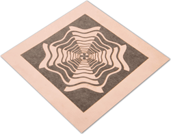
Figure 3 RF antenna structure made using the ProtoMat S103.
The required depth of penetration into the material is well defined in the software and continuously maintained by the Z-axis. This feature ensures secure control of the signal loss and as a result enables the ProtoMat S103 to process substrates with sensitive coatings, such as Rogers 5880. Its precision is shown in Figure 3.
The controlled Z-axis has a stroke of 0.9 inch (22 mm) and extends the plotter's capabilities: it permits the processing of aluminum enclosures. In addition, it can create pockets in rigid printed circuit boards, which prevents the cross-talking of neighboring processors.
Vacuum Table and Camera
Other benefits for RF designers are provided by the vacuum table and the fiducial camera. The vacuum table fixes thin and flexible substrates securely in place while processing, which allows a much higher repeatability than the pass-hole system registry pins. With the vacuum table, prepregs for multilayer production or even PUPI-stencils for solder paste printing can be cut out.
The camera opens up even greater possibilities. For instance, it recognizes fiducials on substrates and calibrates the working result at this location. This allows intermediate processes, so after patterning, the substrate is removed from the ProtoMat, measured and can be connected again for accurate reworking. This is ensured by the vision system with an accuracy of approximately 20 microns for reproccessing and front-to-back alignment. For example, vias or electronic measurements between two patterning steps can be done. Significantly, the reprocessing enables an iterative approach to the prototyping of complex circuitry layouts.
Another innovation becomes relevant when the board is completely structured. For the first time, a ProtoMat model is equipped with a solder paste dispenser. This dispenser uses the integrated camera and locates the solder pads quickly and accurately. In many cases this eliminates a complete step, the printing of solder paste. Ideally, the printed circuit board can be structured and then immediately soldered in the reflow oven.
The ProtoMat S103 is a powerful system for mechanical structuring of RF circuit boards. It is the result of more than 30 years of development and utilizes the capabilities of mechanical processing to the limit. For even higher standards of accuracy and speed, LPKF has also developed the ProtoLaser S, which is a laser system that can structure laminated and ceramic substrates with the help of an IR laser.
LPKF Laser & Electronics AG
Garbsen, Germany
+49 5131 7095-0
www.lpkf.com
