A chain is only as strong as its weakest link and an RF measurement is only as reliable as the most uncertain component or practice. Increasing complexity of communication schemes are driving stringent performance requirements of today’s RF components and networks. The vector network analyzer (VNA) is the instrument of choice for many RF measurements, including high volume semiconductor test systems in both validation and production environments. To fully realize the benefits of a VNA, one must understand the weaknesses of the measurement and correct for them where possible. In this article, four common sources of weakness encountered when using a VNA are covered and recommendations on how to best mitigate or remove these weak links from the measurements are presented.
Correct for Systematic Errors
A discussion around network analyzer operation would not be complete if it did not include a heavy dose of calibration theory and methods. While understanding the calculations and error models behind system calibration can enable one to further improve the accuracy of the measurements, this article will focus more on the basic sources of error in an RF measurement and how to correct for them when possible.

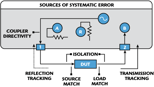
Figure 1 Sources of systematic error can be corrected during a user calibration.
All RF instruments, including network analyzers, require a periodic factory calibration to be performed by a certified calibration laboratory. These calibrations are typically performed yearly and ensure that the network analyzer meets the published specification. They also allow for adjustments to be made when damage or the changing physical characteristics of the VNA over time alter the expected performance. In the RF lab, a dynamic measurement environment creates its own unique challenges, introducing both random and systematic errors. Random sources of error, by definition, are not repeatable or predictable. They can typically be reduced by narrowing the IF bandwidth settings and through averaging. The key to the exceptional measurement accuracy achieved by network analyzers hinges on frequently performing a user calibration to reduce the systematic sources of error. Figure 1 shows a simplified block diagram of a two-port, one-path T/R test set VNA and the sources of systematic error that can be corrected for during a properly performed user calibration.
Systematic Errors
Transmission and Reflection Tracking - Frequency response errors, or transmitted and reflected signal loss, result across all frequencies and must be characterized and corrected.
Source and Load Mismatch - Many RF systems have a characteristic impedance of 50 ½. To properly measure the impedance of the device under test (DUT), any difference between this characteristic impedance and the impedance of the test port, or more specifically, the reference plane, must be accounted for.
Isolation - Errors can occur from crosstalk between various components in the test setup, VNA ports, and measurement reference planes. When this error is significant, it should also be included in the calibration procedure.
Coupler Directivity - VNAs rely on directional elements, often couplers, to separate the transmitted signals from the reflected signals. Ideally, a directional coupler would measure only the forward or reverse traveling signals and produce no output for signals traveling in the opposite direction. Because this is never the reality, the error introduced by coupler leakage must be measured and corrected.
To correct for these systematic errors, one performs a user calibration and measures a set of known stan-dards, compares the measured value to the value of the known standard to calculate the error for each data point, and finally applies the appropriate error correction for each frequency point in the measurement. There is a long list of well-defined, industry standard calibration kits ranging from broadband short, open, load, through (SOLT) standards, suitable for RF frequencies, to transmit-reflect-line (TRL) kits when high accuracy over a narrow bandwidth is required. Additionally, automatic calibration modules are becoming increasingly popular, especially for automated network analysis in validation and production test. In production, maintaining high throughput is so important and excessive time spent calibrating can be costly.
Many factors determine how often a user calibration is performed, including the required measurement accuracy, environmental conditions, and repeatability of the DUT connection. A fresh user calibration may be necessary hourly or weekly. One should use verification standards to determine how often to calibrate. A less stringent practice of measuring a “golden DUT” to determine how often to calibrate can also be used when accuracy requirements are more relaxed.
Throw Out Bad Cables and Adapters
Disposable is typically a word used to describe napkins and dental floss, so it understandably makes us cringe to think about throwing out the cables and adapter sets that carry pricetags easily exceeding a few months rent. Notwithstanding, RF cables and adapters must be regarded as disposable. Designing and producing high quality RF systems depends on the high measurement accuracy of the VNA; a weak or damaged cable or adapter compromises the result and should be discarded. This is simply a part of the expense of making highly accurate measurements.

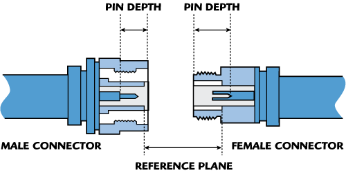
Figure 2 Proper care can extend the life and reliability of expensive cables and adapters.
Figure 2 breaks down a basic connector pair and calls out the important mating elements. By understanding how these connectors are meant to mate and operate, there are a number of ways one can extend the life of cables and connectors.
In addition to meticulous connector care, automatic calibration kits can be used to extend the life of RF adapters and cables. All RF cables and adapters are rated for a limited number of connections. With an automatic calibration module, only one connection is performed during calibration rather than the five to ten connections required for a comparable manual calibration.
Cable Care
Use proper torque - To avoid damage to the connector threads and, more importantly, the center pin, always use a torque wrench adjusted to the appropriate torque when tightening 2.92Êmm, 3.5Êmm, and SMA connectors while finger-tightening N-type connectors.
Frequently gauge the pin depth - Before mating a connector with another device or cable, measure the pin depths of the connectors using a calibrated pin depth gauge. Mating connectors with a pin that is too long will result in damage and compromised measurement results. Mating connectors with a pin that is too short, on the other hand, will degrade the measurement accuracy.
Tighten connectors without rotating the center pin - Never tighten the connectors, adapters, or cables such that the center pin rotates. A rotating center pin creates friction within the connector that can introduce tiny metal shavings into the connector and cause other mechanical alterations and, consequently, change the RF performance.
Avoid mechanical shock - Mechanical shock significantly reduces the connectors' service life. Handle the connectors carefully and avoid dropping them or storing them loosely in a drawer.
Regularly clean connectors - Avoid touching connector mating planes with bare hands as natural skin oils and microscopic dirt particles are difficult to remove. Even in very clean environments, there will be dirt and other debris introduced to the test system, so regularly clean the connectors with compressed air, foam swabs and alcohol.
Properly store connectors - When not in use, keep the connectors covered with their protective dust caps.

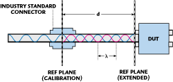
Figure 3 Test fixtures are commonly used for automated semiconductor test. The DUT can be isolated from the test fixture by performing a reference plane extension.
Mind Your Reference Plane
In a VNA measurement, the reference plane is the location in the system where the user calibration is perfomed and, therefore, is the plane from which the measurement is being made. When calibrating a VNA using the SOLT method, for example, attaching the calibration standards to the ends of the cables that are connected to ports 1 and 2 establishes the end of those cables as the reference plane. As shown in Figure 3, any adapters or a test fixture placed between those cables and the DUT are included as part of the measurement and can dramatically alter the results. Consider a 6 GHz sine wave with a 5 cm wavelength, even a single millimeter difference in the actual and desired reference plane results in 7.2 degrees of phase error. When testing semiconductor components and RFICs an industry standard connector such as 2.92 or 3.5 mm, cannot be used, and test fixtures are always used in some fashion in order to connect to the DUT.
The use of a test fixture makes it necessary to use some method of de-embedding to isolate the DUT from the test fixture or the manufacture of custom calibration standards that connect to the test fixture in the same way as the DUT. When it is not feasible to create custom calibration standards matching the test setup, there are a variety of de-embedding techniques that can be used to extend the reference plane of the measurement. Two common and simple approaches to this are time domain gating and reference plane extensions.
Reference Plane Extensions – One can move the reference plane after calibration either automatically or manually. To automatically move the reference plane after calibration, insert an open or short calibration standard at the location in the test setup where the reference plane will be relocated. A crude open can be created, with certain accuracy limitations, by simply removing the DUT from the test system. Figure 3 shows the full reflection that is measured by the VNA when the DUT is replaced by an open or short standard. The VNA can then perform the calculations necessary to move the reference plane and adjust subsequent measurements to match the desired measurement setup. For increased accuracy, one can use a VNA to characterize the test fixture and manually enter the values for trace length and frequency-specific loss. These are then removed (or added) to the measurement to relocate the reference plane.
Time Domain Gating – A VNA makes measurements in the frequency domain and then performs an inverse fast Fourier transform (FFT) to display the response in the time domain. This opens up a wide range of applications including time domain gating. By observing the varying impedance values through an RF signal chain, various components in the system can be identified (in time and distance). Figure 4 shows that by gating only the desired components in the time domain and converting the data back to the frequency domain, the magnitude and phase response of only the DUT, and not the fixture or any additional adapters, can be estimated.

Figure 4 The response of the DUT (blue) is estimated (yellow) by using time domain gating to remove the additional response of a test fixture (green).
Don’t Be the Weakest Link
After taking special care to ensure that the instrument and test setup are properly calibrated and understood, it would be a shame to let poor measurement practices limit the accuracy and reliability of the results. In this way, the engineer becomes a part of the error model, and even the best network analyzer can be quickly rendered ineffective by human error. For example, if proper torque is not used, the repeatability of the measurement and validity of the result are compromised.
It is easy to fall in the trap of adjusting the settings of your VNA until the expected results are achieved. Oftentimes, however, the expected results can differ significantly from the correct result and allow components that operate outside of the design specifications to pass through unnoticed. Following a well-developed process can ensure best practices are adhered to and dramatically improve the reliability and repeatability of the results. This recommended process can be tailored to specific needs and applied to the network analysis to ensure that consistent results are achieved.
VNAs are indispensible tools for accurately measuring the magnitude and phase response of complex RF networks. By understanding the weaknesses of a RF network analysis system, one can ensure that a weak link does not prevent achievement of highly accurate and repeatable VNA measurements.
