The consumer wireless market has seen a “rebirth” of sorts in the last few years, as new data-hungry, mobile devices infiltrate the market and compete for bandwidth on the network. The resurgence in WiFi has been in large part due to the inability of the cellular network to keep up with this demand and provide a back-up solution to users who require always-on network connectivity. All of this has placed a greater emphasis on a key system in these mobile devices known as the “RF front-end.”

Figure 1 Simplified block diagram of a typical wireless RF front-end.
The RF front-end is a set of components in a mobile device, which functionally sits between the antenna and the wireless transceiver. Its job is to close the radio link (transmit and receive) between the user and the network and maintain that link as the user goes about his daily activities. A simplified block diagram of an RF front-end is shown in Figure 1.
The transition into 3G/4G and the requirement to maintain compatibility with legacy networks has necessitated that mobile devices support multi-mode/multi-band (MMMB) operation. This has significantly increased the complexity of the front-end in relation to the rest of the electronics in the radio. Statistics suggest that greater than 50 percent of all cellular handsets past 2011 will support three or more frequency bands1 in order to support this transition. These new “smart phones” are achieving a level of complexity that likely rivals sophisticated military radios of several years ago and are entering an era when the demand for performance, reduced complexity and lower cost are all driving a move toward silicon-based technologies.
Until now, the development of these RF front-ends has relied on III-V technologies for the majority of the functionality, with CMOS and passives technologies playing a lesser role. The III-V’s cut their teeth during the late 1970s and early 1980s, as the darling technology of the defense industry and became more mainstream in the 1990s, as they were applied to more consumer-oriented applications. They provide a very good combination of power density, reverse breakdown, ft and isolation, all of which are key figures of merit when addressing the RF front-end application space.
As radio complexity increases, cost becomes a major factor and drives the need to seek alternative architectures or technologies. Published work2-4 on advancements in silicon-based technologies and specifically silicon-on-insulator (SOI) technologies, suggest that silicon can provide competitive performance to traditional III-V’s with the added advantages of lower cost, greater integration capability and virtually unlimited capacity. Moreover, the differentiating features these silicon technologies provide can lead to innovative architectures and solutions, which help in rethinking traditional approaches.

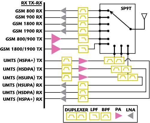
Figure 2 Block diagram of a quad-band EDGE/tri-band UMTS cellualar front-end components.
As shown in Figure 2, a MMMB smart phone can have several GSM and UMTS/WCDMA bands, whose transmit and receive chains are hooked up into an antenna through a single-pole nine-throw switch (SP9T). Today’s solution for this FE includes several power amplifier modules (PAM), a switch module, and several discrete filters. This complexity can quickly grow in future smart phones and needs to be addressed by integration for lower cost and a smaller form factor. Fundamentally, this is an opportunity for silicon technologies that have demonstrated capability in switches and power amplifiers. Several areas where SOI is addressing functionality in the RF front-end, specifically the switch, the PA and the LNA, will be explored.
RF Switch Solutions
In the context of RF switches, minimizing insertion loss (IL) and maximizing isolation (ISO) is a concern, while maintaining low harmonics. To support GSM power levels in a low voltage CMOS technology, numerous FETs in a series or a shunt branch must be stacked. The optimization of IL and ISO then depends on the number of FET stack and the width of the FET in the switch branch, which has been discussed previously.2
The SOI technology uses a 2.5 V NFET in the 180 nm process as described by Botula et al,3 which has demonstrated a capability to attain a Ron Coff of 250 fs. Single-pole single-throw switch branches, built with 12-stack FETs with each FET having 4 mm width, show second and third harmonics levels of -67 dBm and -59 dBm, respectively, in the OFF mode. Further investigation is under way to improve the Ron Coff product, while maintaining low harmonics and high reliability.
Switch branches were arranged in a series-shunt combination to design an SP8T switch.4 An RF measurement at 890 MHz and 35 dBm input power on port-6 to antenna shows that an IL of 0.8 dB can be achieved, with a P2fo at -50 dBm, and P3fo at -58 dBm. The IIP2 measured using a 1829 MHz blocker frequency shows 108 dBm. IIP3 measured higher than 66 dBm for all bands. These results are quite compelling to meet many product applications.
Power Amplifier Solutions
The PAs are one of the highest power consuming elements in the radio and poses a formidable challenge for FEM integration. Highly efficient and linear PAs are desirable to make sure that the talk time and data throughput are maximized. The RF output power obtained from a transistor is directly proportional to the square of the output voltage delivered to the load impedance. A higher breakdown voltage device can, therefore, more easily provide the required output power and would be capable of improved robustness. In the context of PA technologies, several previous works have compared the performance of GaAs HBT, Si BJT, SiGe HBT, and n-MOSFET.5, 6 It can be observed that while silicon technologies are not the best in class, the silicon based transistors are very capable to achieving the cellular PA performance targets by careful layout and design considerations.

Figure 3 500 μm 2.5 V NFET DC IV curves with load line.
A 2.5 V NFET, with a BVdss, approaching 5 V is available in this technology, which has an Ron / ft / fmax performance similar to a switch optimized device. Several single stage common source 2.5 V NFET power cell structures were load-pulled with second and third harmonic load matching. Figure 3 shows a 1.95 GHz operating area, overlaid on the DC IV, curve for a 500 µm device biased and impedance matched for maximum class AB output power. This device can operate in a safe operating area up to 3.6 V on the drain. It was noted that the load line became more oval shaped as the fundamental and harmonic load matching was moved from 50 Ω to the optimal Pout matching. This device obtained a 1 dB compressed output power of 16 dBm with a gain of 16 dB and an efficiency of 66 percent.

Figure 4 5 mm 2.5 V NFET load-pull optimized for PAE.
Figure 4 shows a load-pull plot for a 5 mm total gate width structure, which produced a Pout of 22.5 dBm and a gain of 10 dB at the peak PAE of 63.7 percent. The measured IM3 was based on a 1 MHz tone spacing. Backing off by 6 dB to a Pout of 16.5 dBm for a more linear operation, shows that this device measured a gain of 14 dB, an IM3 of -14 dBm and a PAE of 31 percent. These results demonstrate that a CMOS based power amplifier solution for RF applications can be made a reality in SOI processes.
Low Noise Amplifier Solutions

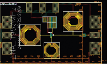
Figure 5 1.95 GHz LNA layout with on-chip matching.
Low noise amplifiers, having low power consumption, yet requiring high Q matching components to maintain a low noise figure, can be ideal to integrate on the same SOI device as the switch. The 1.8 V 180 nm nfet provides sufficient gain and high enough compression for the cellular and WLAN frequency bands. Thick Cu metallization, placed further away from the substrate, allows for high-Q inductors. A simple cascode LNA, which was optimized at 1.95 GHz for model to hardware correlation, is used to demonstrate its feasibility. The layout, including on chip matching and probe pads, is shown in Figure 5. The dimensions, excluding the pads, are 500 × 360 µm.
An example of the high Q achievable on this process is the inductor on the left, which is a 7.5 turns 160 µm diameter, 5 µm wide, octagon that provides 8.74 nH and a Q of 15.1, peaking at 2.95 GHz for the input match. Biasing this LNA, at 1.5 V and 3 mA, provides 12.4 dB of gain, a noise figure (NF) of 1.7 dB and an input P1dB of -8 dBm, while maintaining a return loss better than 15 dB for both ports. Increasing the current to 6.5 mA will increase the gain and P1dB to 13.7 dB and -2 dBm, respectively, and decrease the NF to 1.4 dB.
Conclusion
SOI technology solutions are becoming well positioned for FEM integration in advanced wireless communication systems. Today, SOI CMOS provides a cost-effective solution for RF switches. Obtaining the necessary LNA performance is easily achieved in SOI because of the low loss substrate positive effect on matching and the active devices. With progressive advancement in cellular PA SOI solutions, the pathway for further FEM integrated solutions can soon be a market reality.
Acknowledgment
The authors wish to acknowledge the assistance and support of various groups within IBM for the success of various FEM technologies and testing.
References
- “RF Device/Module for Cellular 2009/2010,” Navian Inc. Report 2010.1.5 http://www.navian.co.jp/summaries/Sample_RF09_English_Ver.pdf.
- A. Joseph, P. Gammel, P. Rabbeni, R. Wolf and J. Dunn, “Silicon Solutions for Front-end Applications,” 2011 IEEE Topical Meeting on Silicon Monolithic Integrated Circuits in RF Systems Digest, pp. 109-112.
- A. Botula, A. Joseph, J. Slinkman, R. Wolf, Z-X. He, D. Ioannou, L. Wagner, M. Gordon, M. Abou-Khalil, R. Phelps, M. Gautsh, W. Abadeer, D. Harmon, M. Levy, J. Benoit and J. Dunn, “A Thin-Film SOI 180 nm CMOS RF Switch Technology,” 2009 IEEE Topical Meeting on Silicon Monolithic Integrated Circuits in RF Systems Digest,” pp. 1-4.
- D. Wang, R. Wolf, A. Joseph, A. Botula, P. Rabbeni, M. Boenke, D. Harame and J. Dunn, “High Performance SOI RF Switches for Wireless Applications,” 2010 IEEE International Conference on Solid-State and Integrated Circuit Technology Digest, pp. 611-614.
- K. Nellis and P. Zampardi, “A Comparison of Bipolar Technologies for Linear Handset Power Amplifier Applications,” 2003 Proceedings of the IEEE Bipolar/BiCMOS Circuits and Technology Meeting, pp. 3-6.
- D. Milosevic, J.V.D. Tang and A. Roermun, “Investigation on Technological Aspects of Class E RF Power Amplifiers for UMTS Applications (2002),” http://citeseerx.ist.psu.edu/viewdoc/summary?doi=10.1.1.6.3535.
